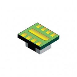
Image shown is a representation only.
Exact specifications should be obtained from the product data sheet.
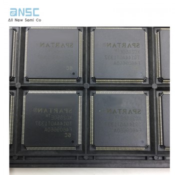
You can contact me for the best price Hot sale original XC2S50E-6FT256C
You can contact me for the best price Hot sale original XC2S50E-6FT256C
|
ANSC PART# |
ANSC- XC2S50E-6FT256C |
|
Part# |
XC2S50E-6FT256C |
|
Type: |
/ |
|
Manufactor |
XILINX |
|
DC |
new |
|
Mount
|
Surface Mount
|
|
Mounting Type
|
Surface Mount
|
|
Package / Case
|
256-LBGA
|
|
Number of Pins
|
256
|
|
Operating Temperature
|
0°C~85°C TJ
|
|
Packaging
|
Tray
|
|
Series
|
Spartan®-IIE
|
|
Published
|
2001
|
|
JESD-609 Code
|
e1
|
|
Pbfree Code
|
yes
|
|
Part Status
|
Obsolete
|
|
Moisture Sensitivity Level (MSL)
|
3 (168 Hours)
|
|
Number of Terminations
|
256
|
|
ECCN Code
|
EAR99
|
|
Terminal Finish
|
Tin/Silver/Copper (Sn95.5Ag4.0Cu0.5)
|
|
HTS Code
|
8542.39.00.01
|
|
Voltage - Supply
|
1.71V~1.89V
|
|
Terminal Position
|
BOTTOM
|
|
Terminal Form
|
BALL
|
|
Peak Reflow Temperature (Cel)
|
260
|
|
Supply Voltage
|
1.8V
|
|
Terminal Pitch
|
1mm
|
|
Frequency
|
357MHz
|
|
Time@Peak Reflow Temperature-Max (s)
|
30
|
|
Base Part Number
|
XC2S50E
|
|
Pin Count
|
256
|
|
Number of Outputs
|
182
|
|
Operating Supply Voltage
|
1.8V
|
|
Number of I/O
|
182
|
|
RAM Size
|
4kB
|
|
Programmable Logic Type
|
FIELD PROGRAMMABLE GATE ARRAY
|
|
Number of Logic Elements/Cells
|
1728
|
|
Total RAM Bits
|
32768
|
|
Number of Gates
|
50000
|
|
Number of LABs/CLBs
|
384
|
|
Speed Grade
|
6
|
|
Combinatorial Delay of a CLB-Max
|
0.47 ns
|
|
Number of CLBs
|
384
|
|
Number of Equivalent Gates
|
23000
|
|
Length
|
17mm
|
|
Height Seated (Max)
|
2mm
|
|
Width
|
17mm
|
|
Radiation Hardening
|
No
|
|
RoHS Status
|
RoHS Compliant
|
|
Lead Free
|
Lead Free
|
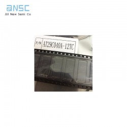
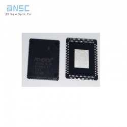
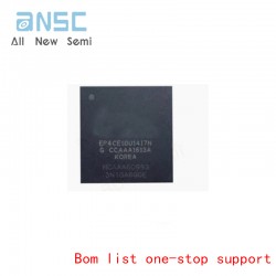
Actual image of the product


You can contact me for the best price Hot sale original XC2S50E-6FT256C
SEND
RFQ