Free hotline:
86-755-88844016
+852 2632 9637
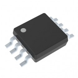
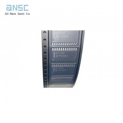
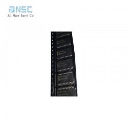
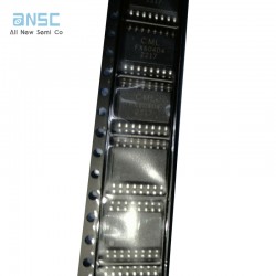
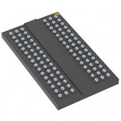
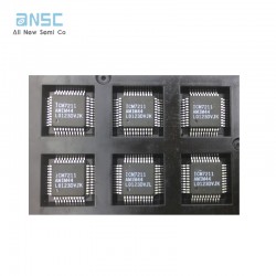
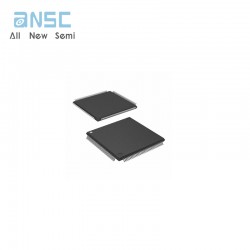
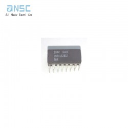
Image shown is a representation only.
Exact specifications should be obtained from the product data sheet.
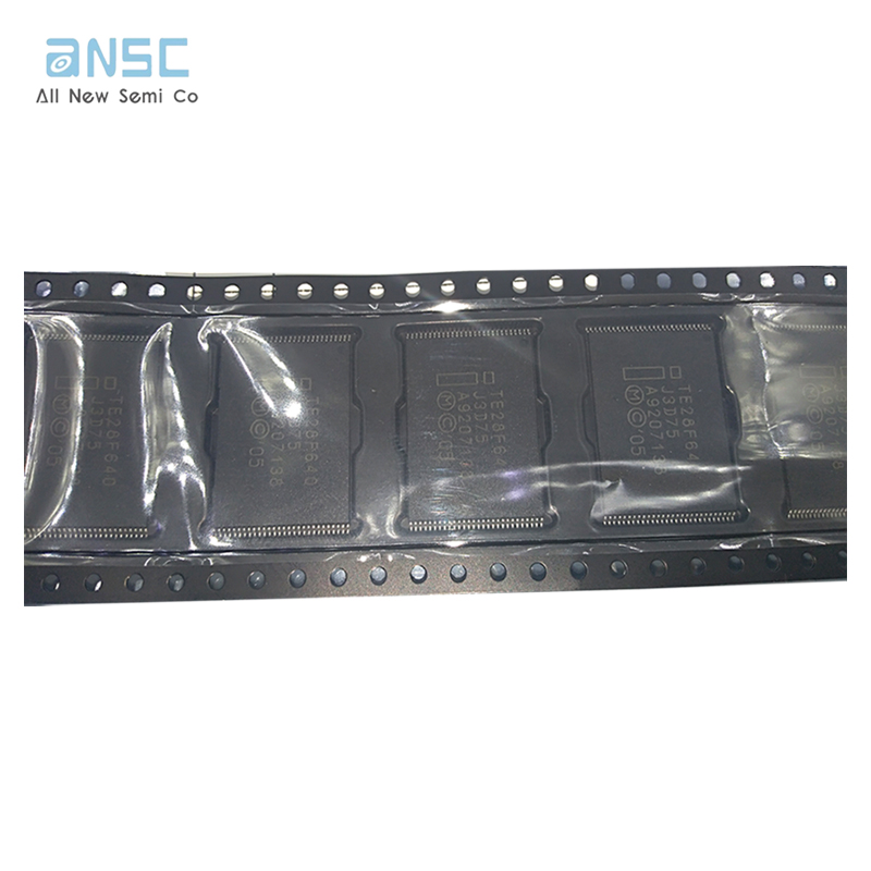
Hot sale original electronics INTEL TE28F640J3D75 Flash, 4MX16, 75ns, PDSO56, 14 X 20 MM, TSOP-56 Unclassified
INTEL TE28F640J3D75 Flash, 4MX16, 75ns, PDSO56, 14 X 20 MM, TSOP-56 Unclassified
Product Details
Introduction
This document contains information pertaining to the Numonyx™ Embedded Flash Memory (J3 v D) device features, operation, and specifications.
Product Features
■ Architecture
— Symmetrical 128-Kbyte blocks
— 256 Mbit (256 blocks)
— 128 Mbit (128 blocks)
— 64 Mbit (64 blocks)
— 32 Mbit (32 blocks)
■ Performance
— 75 ns Initial Access Speed (32,64,128 Mbit densities)
— 95 ns Initial Access Speed (256Mbit only)
— 25 ns 8-word and 4-word Asynchronous page-mode reads
— 32-Byte Write buffer; 4 µs per Byte Effective programming time
■ System Voltage
— VCC = 2.7 V to 3.6 V
— VCCQ = 2.7 V to 3.6 V
■ Packaging
— 56-Lead TSOP (32, 64, 128, 256 Mbit)
— 64-Ball Numonyx Easy BGA package (32, 64, 128 and 256 Mbit)
■ Security
— Enhanced security options for code protection
— 128-bit Protection Register: 64-bits Unique device identifier bits 64-bits User-programmable OTP bits
— Absolute protection with VPEN = GND
— Individual block locking
— Block erase/program lockout during power transitions
■ Software
— Program and erase suspend support
— Flash Data Integrator (FDI), Common Flash Interface (CFI) Compatible
■ Quality and Reliability
— Operating temperature: -40 °C to +85 °C
— 100K Minimum erase cycles per block
— 0.13 µm ETOX™ VIII Process technology
Product Description
|
ANSC PART# |
ANSC- TE28F640J3D75 |
|
Part# |
TE28F640J3D75 |
|
Type: |
Integrated Circuits |
|
Manufactor |
INTEL |
|
DC |
new |
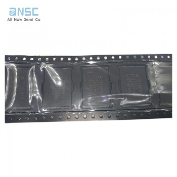
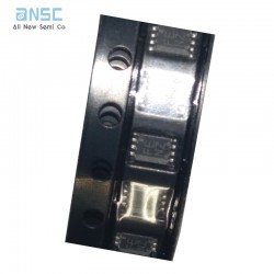
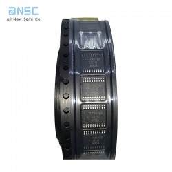
Actual image of the product
Product datasheet
For more information, please download
Payment&Transportation

Official Certificate&Certificate

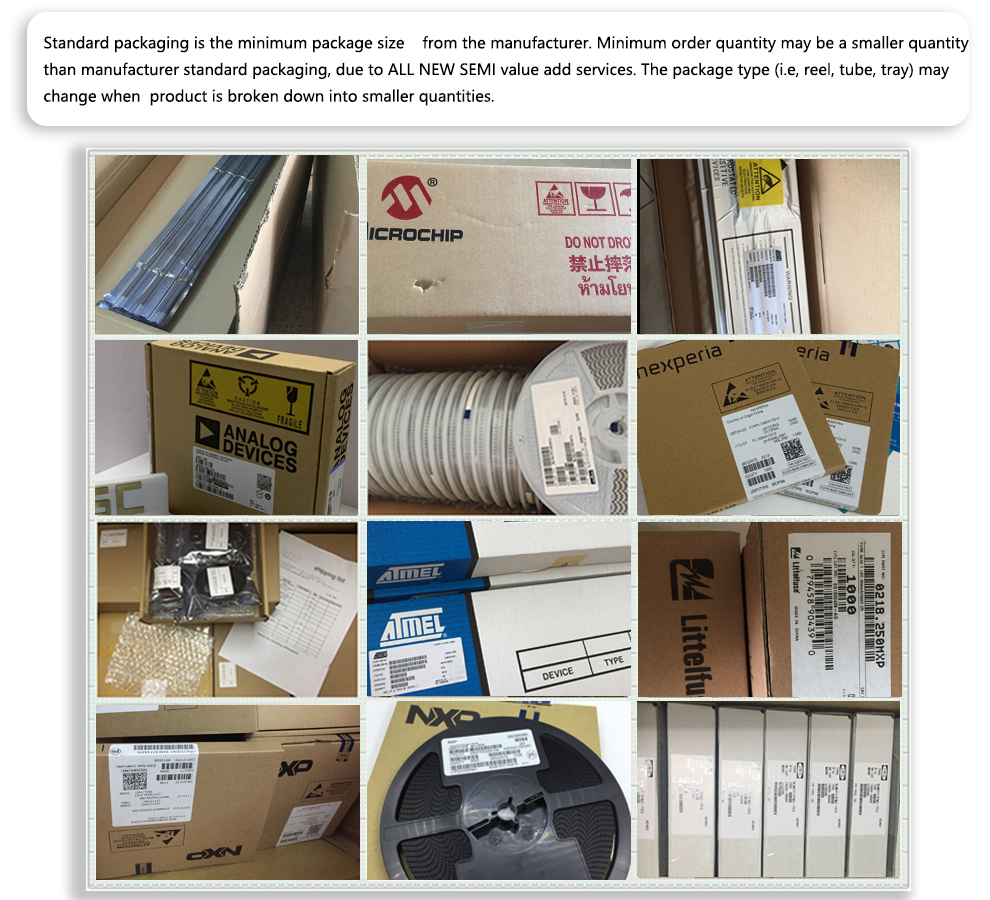
Standard packaging
Multiple product supply
Welcome to visit our company

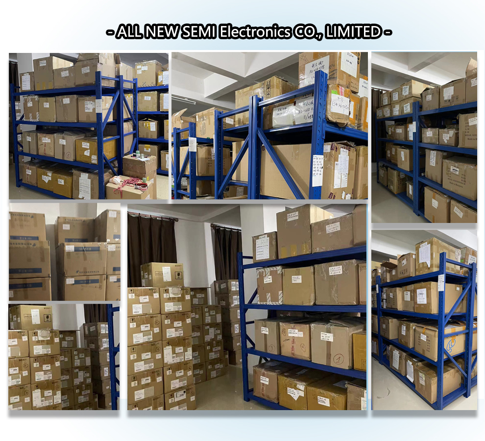
Warehouse Real Shot
