
+86 135 5637 6665
+852 2632 9637

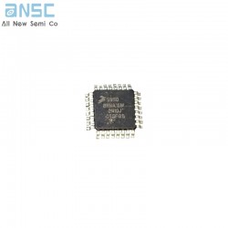
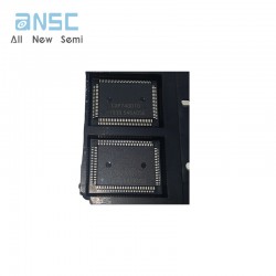
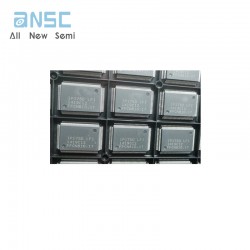
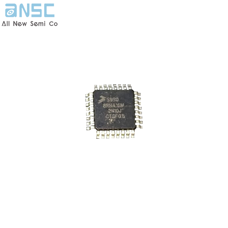
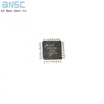
Image shown is a representation only.
Exact specifications should be obtained from the product data sheet.
Integrated circuit
140 MSPS Maximum Conversion Rate
500 MHz Analog Bandwidth
0.5 V to 1.0 V Analog Input Range
400 ps p-p PLL Clock Jitter
Power-Down Mode
3.3 V Power Supply
2.5 V to 3.3 V Three-State CMOS Outputs
Demultiplexed Output Ports
Data Clock Output Provided
Low Power: 570 mW Typical
Internal PLL Generates CLOCK from HSYNC
Serial Port Interface
Fully Programmable
Supports Alternate Pixel Sampling for Higher- Resolution Applications
RGB Graphics Processing
LCD Monitors and Projectors
Plasma Display Panels
Scan Converters
The AD9884A is a complete 8-bit 140 MSPS monolithic analog interface optimized for capturing RGB graphics signals from personal computers and workstations. Its 140 MSPS encode rate capability and full-power analog bandwidth of 500 MHz supports display resolutions of up to 1280 × 1024 (SXGA) at 75 Hz with sufficient input bandwidth to accurately acquire and
digitize each pixel.
To minimize system cost and power dissipation, the AD9884A includes an internal 1.25 V reference, PLL to generate a pixel clock from HSYNC, and programmable gain, offset and clamp circuits. The user provides only a 3.3 V power supply, analog input, and HSYNC signals. Three-state CMOS outputs may be powered by a supply between 2.5 V and 3.3 V.
The AD9884A’s on-chip PLL generates a pixel clock from the HSYNC input. Pixel clock output frequencies range from20 MHz to 140 MHz. PLL clock jitter is typically 400 ps p-p relative to the input reference. When the COAST signal is presented, the PLL maintains its output frequency in the absence of HSYNC. A 32-step sampling phase adjustment is provided.
Data, HSYNC and Data Clock output phase relationships are always maintained. The PLL can be disabled and an external clock input provided as the pixel clock.
A clamp signal is generated internally or may be provided by the user through the CLAMP input pin. This device is fully programmable via a two-wire serial port.
Fabricated in an advanced CMOS process, the AD9884A is provided in a space-saving 128-lead MQFP surface mount plastic package and is specified over a 0°C to +70°C temperature range.
| ANSM-Attribute | Attribute value |
| Model | AD9884AKS-100 |
| Category | Integrated Circuits (ICs) |
| Power Management (PMIC) | |
| Display Drivers | |
| Manufacturer | - |
| Series | - |
| Packaging | Bag |
| Part Status | Obsolete |
| Display Type | LCD |
| Configuration | - |
| Interface | Analog |
| Digits or Characters | - |
| Current - Supply | 125 mA |
| Voltage - Supply | 3V ~ 3.6V |
| Operating Temperature | -20°C ~ 85°C |
| Mounting Type | Surface Mount |
| Package / Case | 128-BFQFP |
| Supplier Device Package | 128-MQFP (14x20) |
| Base Product Number | AD9884 |
Product Data Book:https://allnewsemi.shop/img/cms/IC/AD9884AKS-100.pdf
.jpg)
.png)





Integrated circuit
SEND
RFQ