86-755-88844016
+852 2632 9637
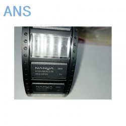
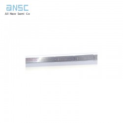
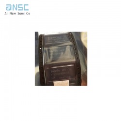
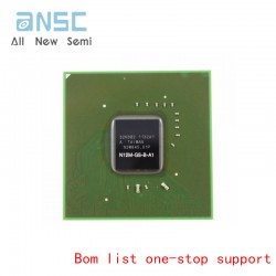
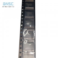
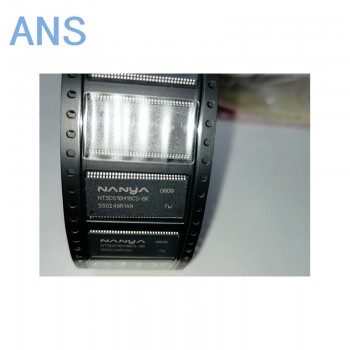
Image shown is a representation only.
Exact specifications should be obtained from the product data sheet.
256Mb DDR Synchronous DRAM 16MX16 0.7ns CMOS TSOP2-66
NT5DS64M4CT, NT5DS32M8CT and NT5DS16M16CT, NT5DS64M4CS, NT5DS32M8CS and NT5DS16M16CS are 256Mb SDRAM devices based using a DDR interface. They are all based on Nanya’s 110 nm design process.
The 256Mb DDR SDRAM uses a double-data-rate architecture to achieve high-speed operation. The double data rate architecture is essentially a 2n prefetch architecture with an interface designed to transfer two data words per clock cycle at the I/O pins. A single read or write access for the 256Mb DDR SDRAM effectively consists of a single 2n-bit wide, one clock cycle data transfer at the internal DRAM core and two corresponding n-bit wide, one-half-clock-cycle data transfers at the I/O pins.
A bidirectional data strobe (DQS) is transmitted externally, along with data, for use in data capture at the receiver. DQS is a strobe transmitted by the DDR SDRAM during Reads and by the memory controller during Writes. DQS is edgealigned with data for Reads and center-aligned with data for Writes.
The 256Mb DDR SDRAM operates from a differential clock (CK and CK; the crossing of CK going high and CK going LOW is referred to as the positive edge of CK). Commands (address and control signals) are registered at every positive edge of CK. Input data is registered on both edges of DQS, and output data is referenced to both edges of DQS, as well as to both edges of CK.
Read and write accesses to the DDR SDRAM are burst oriented; accesses start at a selected location and continue for a programmed number of locations in a programmed sequence. Accesses begin with the registration of an Active command, which is then followed by a Read or Write command. The address bits registered coincident with the Active command are used to select the bank and row to be accessed. The address bits registered coincident with the Read or Write command are used to select the bank and the starting column location for the burst access.
The DDR SDRAM provides for programmable Read or Write burst lengths of 2, 4, or 8 locations. An Auto Precharge function may be enabled to provide a self-timed row precharge that is initiated at the end of the burst access.
As with standard SDRAMs, the pipelined, multibank architecture of DDR SDRAMs allows for concurrent operation, thereby providing high effective bandwidth by hiding row precharge and activation time.
An auto refresh mode is provided along with a power-saving Power Down mode. All inputs are compatible with the JEDEC Standard for SSTL_2. All outputs are SSTL_2, Class II compatible
• DDR 256M bit, die C, based on 110nm design rules
• Double data rate architecture: two data transfers per clock cycle
• Bidirectional data strobe (DQS) is transmitted and received with data, to be used in capturing data at the receiver
• DQS is edge-aligned with data for reads and is centeraligned with data for writes
• Differential clock inputs (CK and CK)
• Four internal banks for concurrent operation
• Data mask (DM) for write data
• DLL aligns DQ and DQS transitions with CK transitions
• Commands entered on each positive CK edge; data and data mask referenced to both edges of DQS
• Burst lengths: 2, 4, or 8
• CAS Latency: 2/2.5(DDR333) , 2.5/3(DDR400)
• Auto Precharge option for each burst access
• Auto Refresh and Self Refresh Modes
• 7.8µs Maximum Average Periodic Refresh Interval
• 2.5V (SSTL_2 compatible) I/O
• VDD = VDDQ = 2.5V ± 0.2V (DDR333)
• VDD = VDDQ = 2.6V ± 0.1V (DDR400)
• Available in Halogen and Lead Free packagin
| Attribute | Attribute value |
| ANSM-Part# | ANSM-NT5DS16M16CS-6K |
| Rohs Code: | Yes |
| Part Life Cycle Code: | Obsolete |
| Ihs Manufacturer: | NANYA TECHNOLOGY CORP |
| Package Description: | TSOP2, TSSOP66,.46 |
| Reach Compliance Code: | unknown |
| Manufacturer: | Nanya Technology Corporation |
| Risk Rank: | 5.13 |
| Access Mode: | FOUR BANK PAGE BURST |
| Access Time-Max: | 0.7 ns |
| Additional Feature: | AUTO/SELF REFRESH |
| I/O Type: | COMMON |
| JESD-30 Code: | R-PDSO-G66 |
| JESD-609 Code: | e3 |
| Length: | 22.22 mm |
| Memory Density: | 268435456 bit |
| Memory IC Type: | DDR DRAM |
| Memory Width: | 16 |
| Number of Functions: | 1 |
| Number of Words: | 16777216 words |
| Number of Words Code: | 16000000 |
| Operating Mode: | SYNCHRONOUS |
| Operating Temperature-Max: | 70 °C |
| Organization: | 16MX16 |
| Output Characteristics: | 3-STATE |
| Package Body Material: | PLASTIC/EPOXY |
| Package Equivalence Code: | TSSOP66,.46 |
| Package Shape: | RECTANGULAR |
| Package Style: | SMALL OUTLINE, THIN PROFILE |
| Power Supplies: | 2.5 V |
| Qualification Status: | Not Qualified |
| Refresh Cycles: | 8192 |
| Seated Height-Max: | 1.2 mm |
| Self Refresh: | YES |
| Subcategory: | DRAMs |
| Supply Voltage-Max (Vsup): | 2.7 V |
| Supply Voltage-Min (Vsup): | 2.3 V |
| Technology: | CMOS |
| Temperature Grade: | COMMERCIAL |
| Terminal Finish: | Matte Tin (Sn) |
| Terminal Form: | GULL WING |
| Terminal Pitch: | 0.65 mm |
| Terminal Position: | DUAL |
| Width: | 10.16 mm |
| Clock Frequency-Max (fCLK): | 166 MHz |
| Interleaved Burst Length: | 2,4,8 |
| ECCN Code: | EAR99 |
| HTS Code: | 8542.32.00.24 |
| Part Package Code: | TSOP2 |
| Pin Count: | 66 |
| Peak Reflow Temperature (Cel): | NOT SPECIFIED |
| Moisture Sensitivity Level: | 3 |

Product Data Book:


For more product information, please download the PDF


We also provide :
| Part No | Manufacturer | Date Code | Quantity | Description |
| LM22676ADJ | NS | 19+ | 250 | SOP8 |
| TPS562201DDCR | TI | 22+ | 795500 | SOT23-6 |
| NJG1806K75 | JRC | 22+ | 500000 | DFN6 |
| TLV74318PDQNR | TI | 22+ | 402000 | X2SON-4 |
| NJG1801K75 | JRC | 22+ | 300000 | SMD |
| NJG1804K64 | JRC | 22+ | 300000 | DFN8 |
| LM27761DSGR | TI | 22+ | 151000 | WSON8 |
| TLV62565DBVR | TI | 22+ | 138000 | SOT23-5 |
| TPS613222ADBVR | TI | 22+ | 108000 | SOT23-5 |
| LNK625DG-TL | POWER | 22+ | 100000 | SOP-8 |
| OPA4322AIPWR | TI | 22+ | 100000 | TSSOP14 |
| TLV75528PDRVR | TI | 22+ | 99000 | WSON-6 |
| TPS7A2025PDQNR | TI | 22+ | 78500 | X2SON-4 |
| TLV62568DBVR | TI | 22+ | 72000 | SOT23-5 |
| STM32L051K8U6TR | ST | 22+ | 60000 | QFN32 |
| SKY66421-11 | SKYWORKS | 22+ | 56500 | QFN16 |
| TPS7A1111PDRVR | TI | 22+ | 54000 | WSON6 |
| TLV62569PDDCR | TI | 22+ | 52000 | SOT23-6 |
| TLV62569DBVR | TI | 22+ | 48000 | SOT23-5 |
| TPS23753APWR | TI | 22+ | 40000 | TSSOP14 |
| NB691GG-Z | MPS | 22+ | 30000 | QFN |
| SN74AHC1G02DBVR | TI | 22+ | 27939 | SOT-23 |
| TPS63000DRCR | TI | 22+ | 23238 | VSON10 |
| TLV75533PDRVR | TI | 22+ | 21500 | WSON6 |
| NB687BGQ-Z | MPS | 22+ | 20000 | QFN |
| A3916GESTR-T-1 | ALLEGRO | 22+ | 17150 | QFN-20 |
| TPS62135RGXR | TI | 22+ | 15000 | VQFN11 |
| TLE2022AMDR | TI | 0803+ | 12500 | SOP8 |
| TPS23756PWPR | TI | 22+ | 12000 | HTSSOP-20 |
256Mb DDR Synchronous DRAM 16MX16 0.7ns CMOS TSOP2-66
SEND
RFQ