+86 135 5637 6665
+852 2632 9637
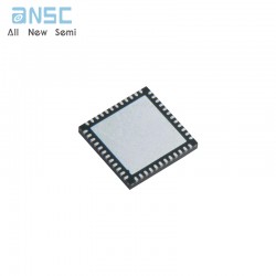
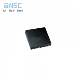
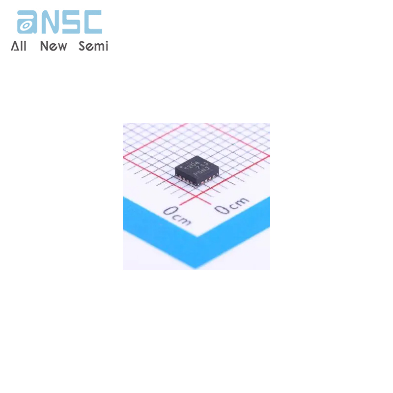
Image shown is a representation only.
Exact specifications should be obtained from the product data sheet.
CDCLVP1204RGTR Four LVPECL Output, High-Performance Clock
The CDCLVP1204 is a highly versatile, low additive jitter buffer that can generate four copies of LVPECL clock outputs from one of two selectable LVPECL, LVDS, or LVCMOS inputs for a variety of communication applications. It has a maximum clock frequency up to 2 GHz. The CDCLVP1204 features an on-chip multiplexer (MUX) for selecting one of two inputs that can be easily configured solely through a control terminal. The overall additive jitter performance is less than 0.1 ps, RMS from 10 kHz to20 MHz, and overall output skew is as low as 15 ps, making the device a perfect choice for use in demanding applications.
The CDCLVP1204 clock buffer distributes one of two selectable clock inputs (IN0, IN1) to four pairs of differential LVPECL clock outputs (OUT0, OUT3) with minimum skew for clock distribution. The CDCLVP1204 can accept two clock sources into an input multiplexer. The inputs can be LVPECL, LVDS, or LVCMOS/LVTTL.
The CDCLVP1204 is specifically designed for driving50-Ωtransmission lines. When driving the inputs in single-ended mode, the LVPECL bias voltage(VAC_REF) must be applied to the unused negative input terminal. However, for high-speed performance up to 2 GHz, differential mode is strongly recommended.
The CDCLVP1204 is characterized for operation from–40°C to +85°C.
• 2:4 Differential Buffer
• Selectable Clock Inputs Through Control Terminal
• Universal Inputs Accept LVPECL, LVDS, and LVCMOS/LVTTL
• Four LVPECL Outputs
• Maximum Clock Frequency: 2 GHz
• Maximum Core Current Consumption: 45 mA
• Very Low Additive Jitter: <100 fs, RMS in 10-kHz to 20-MHz Offset Range:
– 57 fs, RMS (typical) at 122.88 MHz
– 48 fs, RMS (typical) at 156.25 MHz
– 30 fs, RMS (typical) at 312.5 MHz
• 2. 375-V to 3. 6-V Device Power Supply
• Maximum Propagation Delay: 450 ps
• Maximum Output Skew: 15 ps
• LVPECL Reference Voltage, VAC_REF, Available for Capacitive-Coupled Inputs
• Industrial Temperature Range: –40°C to +85°C
• Supports 105°C PCB Temperature (Measured at Thermal Pad)
• ESD Protection Exceeds 2 kV (HBM)
• Wireless Communications
• Telecommunications/Networking
• Medical Imaging
• Test and Measurement Equipment
| Attribute | Attribute value |
| ANSM-Part# | ANSM-CDCLVP1204RGTR |
| Category | Integrated Circuits (ICs) |
| Clock/Timing | |
| Clock Buffers, Drivers | |
| Manufacturer | - |
| Packaging | Tape & Reel (TR) |
| Cut Tape (CT) | |
| Digi-Reel® | |
| Part Status | Active |
| Type | Fanout Buffer (Distribution), Multiplexer |
| Number of Circuits | 1 |
| Ratio - Input:Output | 2:4 |
| Differential - Input:Output | Yes/Yes |
| Input | LVCMOS, LVDS, LVPECL, LVTTL |
| Output | LVPECL |
| Frequency - Max | 2 GHz |
| Voltage - Supply | 2.375V ~ 3.6V |
| Operating Temperature | -40°C ~ 85°C |
| Mounting Type | Surface Mount |
| Package / Case | 16-VFQFN Exposed Pad |
| Supplier Device Package | 16-VQFN (3x3) |
| Base Product Number | CDCLVP1204 |
For more product information, please download the PDF
CDCLVP1204RGTR Four LVPECL Output, High-Performance Clock
SEND
RFQ