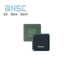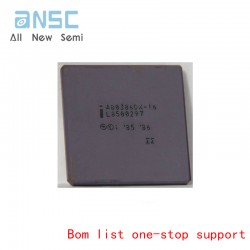
Integrated Circuit
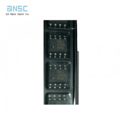
Hot sale original electronics CY8C4125PVI-482 IC MCU 32BIT 32KB FLASH 28SSOP ARM® Cortex®-M0 PSOC® 4
$0.00
86-755-88844016
+852 2632 9637
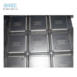
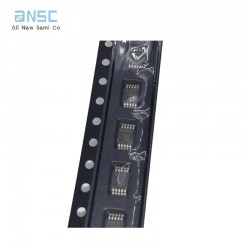
Image shown is a representation only.
Exact specifications should be obtained from the product data sheet.
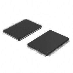
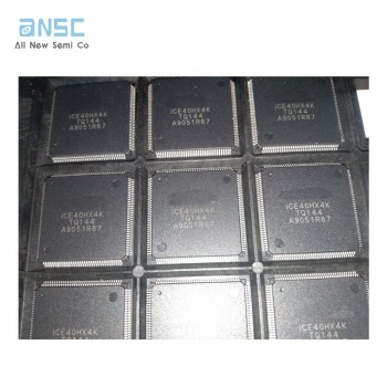
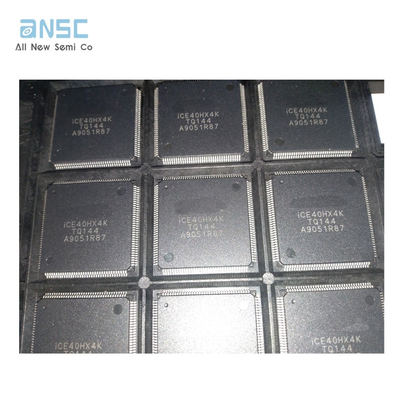
IC FPGA 107 I/O 144TQFP iCE40™ HX Field Programmable Gate Array (FPGA) IC 107 81920 3520 144-LQFP
In the 144-LQFP package, you will find fpga chips. FIELD PROGRAMMABLE GATE ARRAY is the component of this type of FPGA. There are 107 I/Os for better data transfer. Supply voltage is 1.2V volts. There is a Field Programmable Gate Arrays family component in this FPGA part. The Surface Mount-slot on the development board allows you to attach the FPGA module. The supply voltage of the device is 1.14V~1.26V , at which it runs. An FPGA belonging to the iCE40? HX series is referred to as an FPGA. Fpga chips is important to maintain the operating temperature wFpga chipshin the range of -40°C~100°C TJ when operating the machine. A device such as this one has 107 outputs built into it. Fpga chips is designed to maximiTraye space efficiency by containing the FPGA model in Tray. In total, it has 144 terminations on each end. There are 81920 RAM bits that are available with this device. In order to find related parts, you can use its base part number ICE40. For the program to work properly, the RAM si10kBe of this FPGA module must reach 10kB GB in order to ensure normal operation. In this case, there are 144 pins on the board. This FPGA is built as an array of 440 LABs/CLBs. In operation with 1.2V, designers can take advantage of its flexibility to the fullest extent. Programs and data can be stored in the 10kB memory embedded in this FPGA module. During the process of storing and transferring data, 3520 registers are used. A CLB is a basic module that determines the architecture of a system. It is possible to achieve a speed of up to 533MHz with this FPGA.
107 I/Os
Up to 81920 RAM bits
144 LABs/CLBs
3520 registers
There are a lot of Lattice Semiconductor Corporation ICE40HX4K-TQ144 FPGAs applications.
Server Applications
Image processing
Enterprise networking
Medical ultrasounds
Electronic Warfare
Automotive
Camera time adjustments
Distributed Monetary Systems
Computer hardware emulation
Industrial IoT
|
ANSC PART# |
ANSC- iCE40HX4K-TQ144 |
|
Part# |
iCE40HX4K-TQ144 |
|
Type: |
Integrated Circuits(ICs) |
|
Manufactor |
Lattice Semiconductor Corporation |
|
DC |
new |
|
Package / Case |
144-LQFP |
|
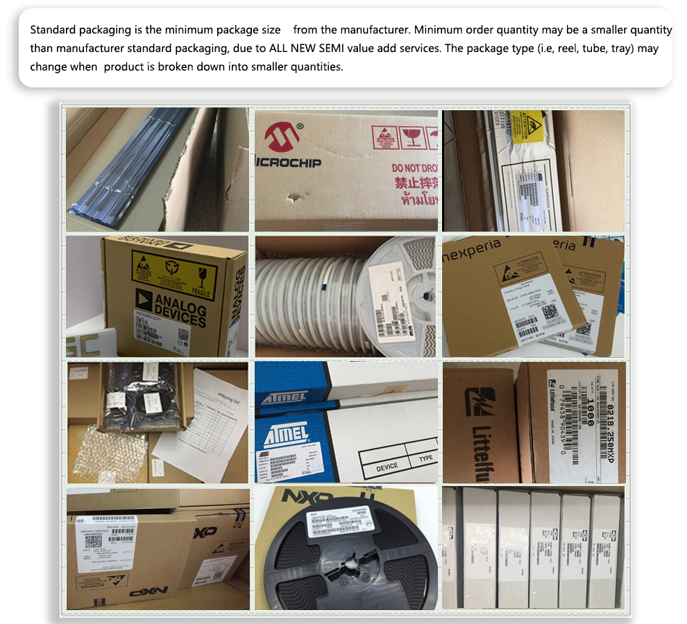
Supplier Device Package |
Tray |
Product Attributes
| TYPE | DESCRIPTION |
| Category | Integrated Circuits (ICs) |
| Embedded | |
| FPGAs (Field Programmable Gate Array) | |
| Mfr | Lattice Semiconductor Corporation |
| Series | iCE40邃「 HX |
| Package | Tray |
| Product Status | Active |
| DigiKey Programmable | Not Verified |
| Number of LABs/CLBs | 440 |
| Number of Logic Elements/Cells | 3520 |
| Total RAM Bits | 81920 |
| Number of I/O | 107 |
| Voltage - Supply | 1.14V ~ 1.26V |
| Mounting Type | Surface Mount |
| Operating Temperature | -40ツーC ~ 100ツーC (TJ) |
| Package / Case | 144-LQFP |
| Supplier Device Package | 144-TQFP (20x20) |
| Base Product Number | ICE40 |
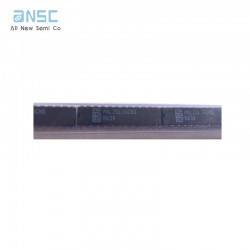
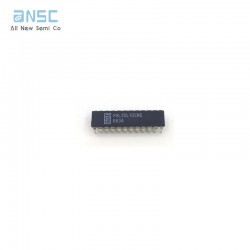
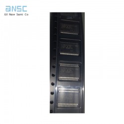
Actual image of the product
Product datasheet
For more information, please download


IC FPGA 107 I/O 144TQFP iCE40™ HX Field Programmable Gate Array (FPGA) IC 107 81920 3520 144-LQFP
SEND
RFQ