
+86 135 5637 6665
+852 2632 9637
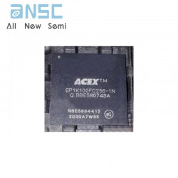
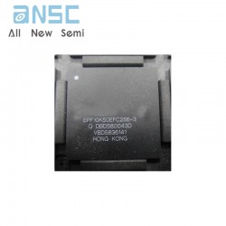
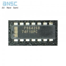
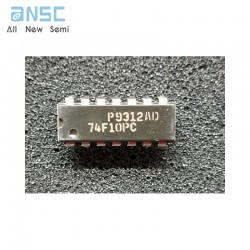
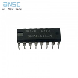
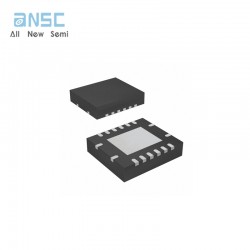
Image shown is a representation only.
Exact specifications should be obtained from the product data sheet.
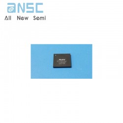
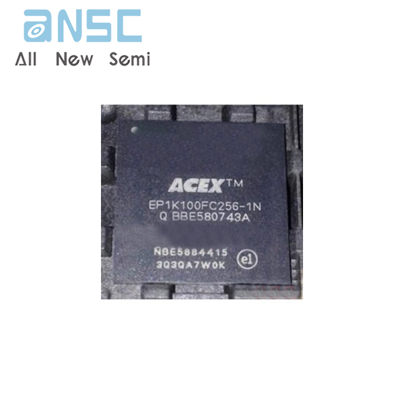
EP1K100FC256-1N Programmable Logic Device Family IC BGA
ACEX 1K devices provide a die-efficient, low-cost architecture by combining look-up table (LUT) architecture with EABs. LUT-based logic
provides optimized performance and efficiency for data-path, register intensive, mathematical, or digital signal processing (DSP) designs, while
EABs implement RAM, ROM, dual-port RAM, or first-in first-out (FIFO) functions. These elements make ACEX 1K suitable for complex logic
functions and memory functions such as digital signal processing, wide data-path manipulation, data transformation and microcontrollers, as
required in high-performance communications applications. Based on reconfigurable CMOS SRAM elements, the ACEX 1K architecture
incorporates all features necessary to implement common gate array megafunctions, along with a high pin count to enable an effective interface
with system components. The advanced process and the low voltage requirement of the 2.5-V core allow ACEX 1K devices to meet the
requirements of low-cost, high-volume applications ranging from DSL modems to low-cost switches.
The ability to reconfigure ACEX 1K devices enables complete testing prior to shipment and allows the designer to focus on simulation and design verification. ACEX 1K device reconfigurability eliminates inventory management for gate array designs and test vector generation for fault coverage.
All performance results were obtained with Synopsys DesignWare or LPM functions. Special design techniques are not required to implement
the applications; the designer simply infers or instantiates a function in a Verilog HDL, VHDL, Altera Hardware Description Language (AHDL), or
schematic design file.
■ Programmable logic devices (PLDs), providing low cost system-on-a-programmable-chip (SOPC) integration in a single device
– Enhanced embedded array for implementing megafunctions such as efficient memory and specialized logic functions
– Dual-port capability with up to 16-bit width per embedded array block (EAB)
– Logic array for general logic functions
■ High density
– 10,000 to 100,000 typical gates (see Table 1)
– Up to 49,152 RAM bits (4,096 bits per EAB, all of which can be used without reducing logic capacity)
■ Cost-efficient programmable architecture for high-volume applications
– Cost-optimized process
– Low cost solution for high-performance communications applications
■ System-level features
– MultiVoltTM I/O pins can drive or be driven by 2.5-V, 3.3-V, or 5.0-V devices
– Low power consumption
– Bidirectional I/O performance (setup time [tSU] and clock-tooutput delay [tCO]) up to 250 MHz
– Fully compliant with the peripheral component interconnect Special Interest Group (PCI SIG) PCI Local Bus Specification, Revision 2.2 for 3.3-V operation at 33 MHz or 66 MHz
■ Extended temperature range
– -1 speed grade devices are compliant with PCI Local Bus Specification, Revision 2.2 for 5.0-V operation
– Built-in Joint Test Action Group (JTAG) boundary-scan test (BST) circuitry compliant with IEEE Std. 1149.1-1990, available without consuming additional device logic.
– Operate with a 2.5-V internal supply voltage
– In-circuit reconfigurability (ICR) via external configuration devices, intelligent controller, or JTAG port
– ClockLockTM and ClockBoostTM options for reduced clock delay, clock skew, and clock multiplication
– Built-in, low-skew clock distribution trees
– 100% functional testing of all devices; test vectors or scan chains are not required
– Pull-up on I/O pins before and during configuration
■ Flexible interconnect
– FastTrack® Interconnect continuous routing structure for fast,
predictable interconnect delays
– Dedicated carry chain that implements arithmetic functions such as fast adders, counters, and comparators (automatically used by software tools and megafunctions)
– Dedicated cascade chain that implements high-speed, high-fan-in logic functions (automatically used by software tools and megafunctions)
– Tri-state emulation that implements internal tri-state buses
– Up to six global clock signals and four global clear signals
■ Powerful I/O pins
– Individual tri-state output enable control for each pin
– Open-drain option on each I/O pin
– Programmable output slew-rate control to reduce switching noise
– Clamp to VCCIO user-selectable on a pin-by-pin basis
– Supports hot-socketing
| Attribute | Attribute value |
| ANSM-Part# | ANSM-EP1K100FC256-1N |
| Category | Integrated Circuits (ICs) |
| Embedded | |
| FPGAs (Field Programmable Gate Array) | |
| Mfr | - |
| Series | ACEX-1K |
| Packaging | Tray |
| Part Status | Obsolete |
| DigiKey Programmable | Not Verified |
| Number of LABs/CLBs | 624 |
| Number of Logic Elements/Cells | 4992 |
| Total RAM Bits | 49152 |
| Number of I/O | 186 |
| Number of Gates | 257000 |
| Voltage - Supply | 2.375V ~ 2.625V |
| Mounting Type | Surface Mount |
| Operating Temperature | 0°C ~ 70°C (TA) |
| Package / Case | 256-BGA |
| Supplier Device Package | 256-FBGA (17x17) |
| Base Product Number | EP1K100 |
For more product information, please download the PDF
EP1K100FC256-1N Programmable Logic Device Family IC BGA
SEND
RFQ