+86 135 5637 6665
+852 2632 9637
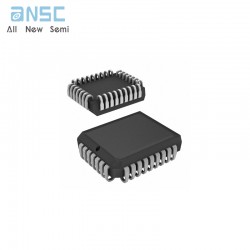
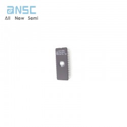
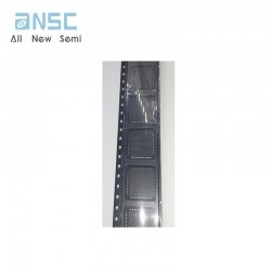
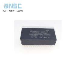
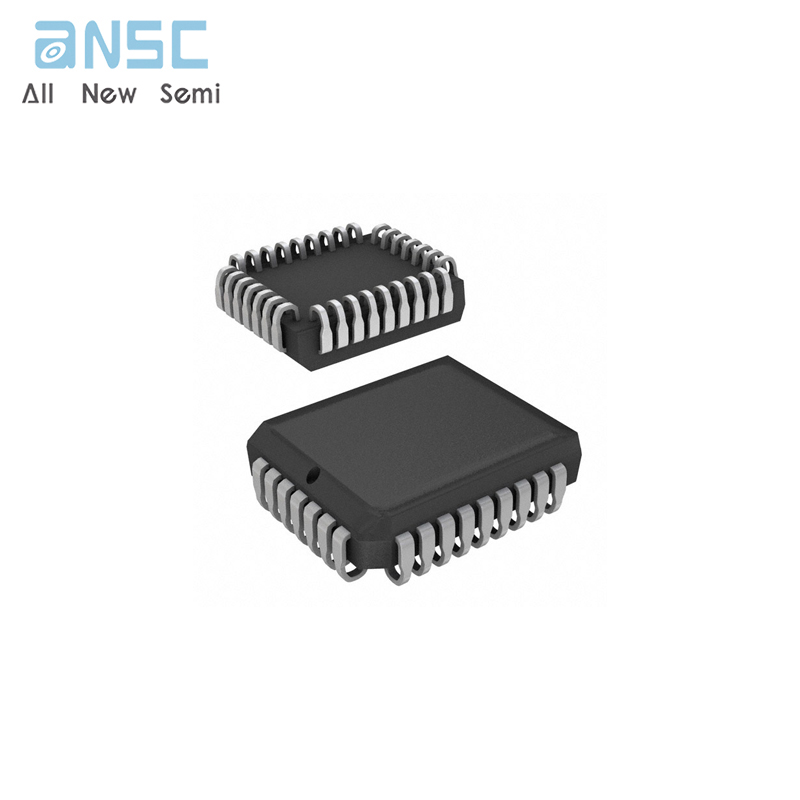
Image shown is a representation only.
Exact specifications should be obtained from the product data sheet.
AT49BV040A-70JI 4-megabit Single 2.7-volt Battery-Voltage Flash Memory PLCC32 spot stock
The AT49BV040A is a 2.7-volt-only in-system reprogrammable Flash Memory. Its4 megabits of memory is organized as 524,288 words by 8 bits. Manufactured with Atmel’s advanced nonvolatile CMOS technology, the device offers access times to70 ns with power dissipation of just 54 mW over the commercial temperature range.
When the device is deselected, the CMOS standby current is less than 50 µA. To allow for simple in-system reprogrammability, the AT49BV040A does not require high input voltages for programming. Three-volt-only commands determine the read and programming operation of the device. Reading data out of the device is similar to reading from an EPROM; it has standard CE, OE , and WE inputs to avoid bus contention. Reprogramming the AT49BV040A is performed by erasing a block of data and then programming on a byte by byte basis. The byte programming time is a fast 30 µs. The end of a program cycle can be optionally detected by the DATA polling feature. Once the end of a byte program cycle has been detected, a new access for a read or program can begin. The typical number of program and erase cycles is in excess of10,000 cycles.
The device is erased by executing the erase command sequence; the device internally controls the erase operations. There are two 8K byte parameter block sections, eight main memory blocks, and one boot block.
The device has the capability to protect the data in the boot block; this feature is enabled by a command sequence. The 16K-byte boot block section includes a reprogramming lock out feature to provide data integrity. The boot sector is designed to contain user secure code, and when the feature is enabled, the boot sector is permanently protected from being reprogrammed.
• Single Supply for Read and Write: 2.7 to 3.6V
• Fast Read Access Time – 70 ns
• Internal Program Control and Timer
• Sector Architecture
– One 16K Bytes Boot Block with Programming Lockout
– Two 8K Bytes Parameter Blocks
– Eight Main Memory Blocks (One 32K Bytes, Seven 64K Bytes)
• Fast Erase Cycle Time – 7 Seconds
• Byte-by-Byte Programming – 30 µs/Byte Typical
• Hardware Data Protection
• DATA Polling for End of Program Detection
• Low Power Dissipation
– 15 mA Active Current
– 50 µA CMOS Standby Current
• Typical 10,000 Write Cycles
• Green (Pb/Halide-free) Packaging Option
| Attribute | Attribute value |
| ANSM-Part# | ANSM-AT49BV040A-70JI |
| Category | Integrated Circuits (ICs) |
| Memory | |
| Memory | |
| Mfr | - |
| Packaging | Tube |
| Part Status | Obsolete |
| DigiKey Programmable | Not Verified |
| Memory Type | Non-Volatile |
| Memory Format | FLASH |
| Technology | FLASH |
| Memory Size | 4Mbit |
| Memory Organization | 512K x 8 |
| Memory Interface | Parallel |
| Write Cycle Time - Word, Page | 50µs |
| Access Time | 70 ns |
| Voltage - Supply | 2.7V ~ 3.6V |
| Operating Temperature | -40°C ~ 85°C (TC) |
| Mounting Type | Surface Mount |
| Package / Case | 32-LCC (J-Lead) |
| Supplier Device Package | 32-PLCC (13.97x11.43) |
| Base Product Number | AT49BV040 |
For more product information, please download the PDF
AT49BV040A-70JI 4-megabit Single 2.7-volt Battery-Voltage Flash Memory PLCC32 spot stock
SEND
RFQ