+86 135 5637 6665
+852 2632 9637
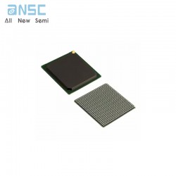
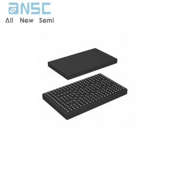
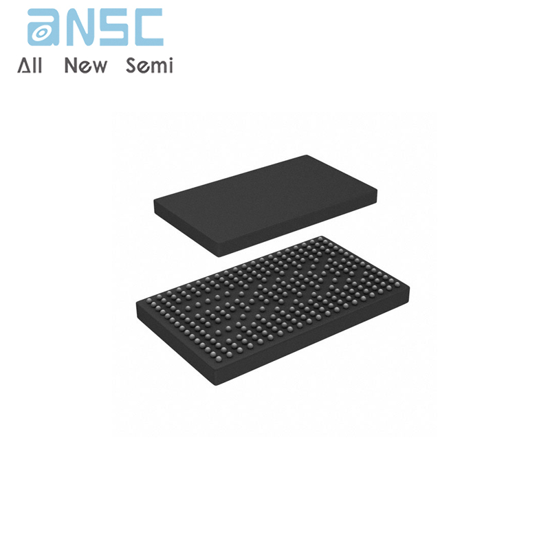
Image shown is a representation only.
Exact specifications should be obtained from the product data sheet.
CAB4AZNRR Command/Address/Control Buffer
The CAB4 is 32-bit 1:2 Command/Address/Control Buffer and 1:4 differential Clock Buffer designed for operation on DDR4 registered DIMMs with a 1.2 V VDD mode.
All inputs are pseudo-differential using external or internal voltage reference. All outputs are full swing CMOS drivers optimized to drive 15 to 50 Ω effective terminated traces in DDR4 RDIMM, LRDIMM and 3D-Stacked DIMM applications. The clock outputs, command/address outputs, control outputs, data buffer control outputs can be enabled in groups, and independently driven with different strengths to compensate for different DIMM net topologies. The DDR4 Register operates from a differential clock (CK_t and CK_c). Inputs are registered at the crossing of CK_t going HIGH, and CK_c going LOW.
The input signals could be either re-driven to the outputs if one of the input signals DCS[n:0]_n is driven LOW or it could be used to access device internal control registers when certain input conditions are met.
The device is characterized in the operating temperature range from -40°C to 95°C.
• DDR4RCD01 JEDEC Compliant
• DDR4 RDIMM and LRDIMM up to DDR4-2400
• 32 Bits 1-to-2 Register Outputs
• 1-to-4 Differential Clock Buffer
• 1.2V Operation
• PLL with Internal Feedback
• Configurable Driver Strength
• Scalable Weak Driver
• Programmable Latency
• Output Driver Calibration
• Address Mirroring and Inversion
• DDR4 Full-Parity Operation
• On-Chip Programmable VREF Generation
• CA Bus Training Mode
• I2C™ Interface Support
• Up to 16-Logical Ranks Support for 3DS RDIMMs and LRDIMMs
• Up to 4 Physical Ranks Support for RDIMMs and LRDIMMS
| Attribute | Attribute value |
| ANSM-Part# | ANSM-CAB4AZNRR |
| Category | Integrated Circuits (ICs) |
| Clock/Timing | |
| Application Specific Clock/Timing | |
| Manufacturer | - |
| Packaging | Tape & Reel (TR) |
| Part Status | Obsolete |
| DigiKey Programmable | Not Verified |
| PLL | No |
| Main Purpose | Memory, DDR |
| Input | CMOS |
| Output | CMOS |
| Number of Circuits | 1 |
| Ratio - Input:Output | 1:4 |
| Differential - Input:Output | Yes/Yes |
| Frequency - Max | 2.4Gbps |
| Voltage - Supply | 1.2V |
| Operating Temperature | -40°C ~ 95°C |
| Mounting Type | Surface Mount |
| Package / Case | 253-LFBGA |
| Supplier Device Package | 253-NFBGA (13.5x8) |
| Base Product Number | CAB4 |
For more product information, please download the PDF
CAB4AZNRR Command/Address/Control Buffer
SEND
RFQ