+86 135 5637 6665
+852 2632 9637
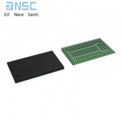
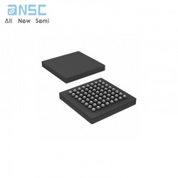
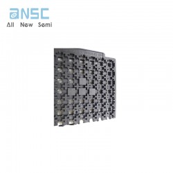
Image shown is a representation only.
Exact specifications should be obtained from the product data sheet.
SSTE32882KB1AKG8 Pinout optimizes DDR3 RDIMM Clock Driver IC BGA spot stock
This 28-bit 1:2, or 26-bit 1:2 and 4-bit 1:1, registering clock driver with parity is designed for 1.25V, 1.35V and 1.5V VDD operation.
All inputs are 1.25,1.35V and 1.5V CMOS compatible, except the reset (RESET) and MIRROR inputs which are LVCMOS. All outputs are 1.25V,1.35V and 1.5V CMOS edge-controlled drivers optimized to drive single terminated 25 to 50 traces in DDR3 RDIMM applications, except the open-drain error (ERROUT) output. The clock outputs (Yn and Yn) and control net outputs QnCKEn, QnCSn and QnODTn are designed with a different strength and skew to compensate for different loading and equalize signal travel speed.
• Pinout optimizes DDR3 RDIMM PCB layout
• DDR3-800/1066/1333/1600/1866/2133 rate
• 1-to-2 Register Outputs and 1-to-4 Clock Pair Outputs support stacked DDR3 RDIMMs
• Phase Lock Loop clock driver for buffering one differential clock pair (CK and CK) and distributing to four differential outputs
• Supports LVCMOS switching levels on the RESET and MIRROR inputs
• Checks priority on DIMM-independent data inputs
• Supports dynamic 1T/3T timing transaction and output inversion feature for improved timing performance during normal operations and MRS command pass-through
• Supports CKE Power Down operation modes
• Supports Quad Chip Select operation features
• RESET input disables differential input recievers, resets all registers, and disables all output drivers except ERROUT and QnCKEn
• Provides access to internal control words for configuring the device features and adapting in different RDIMM and system applications
• Latch-up performance exceeds 100mA
• ESD > 2000V per MIL-STD883, Method 3015; ESD > 200V using machine model (c = 200pF, R = 0)
• Available in 176 Ball Grid Array package
| Attribute | Attribute value |
| ANSM-Part# | ANSM-SSTE32882KB1AKG8 |
| Category | Integrated Circuits (ICs) |
| Clock/Timing | |
| Application Specific Clock/Timing | |
| Manufacturer | - |
| Packaging | Tape & Reel (TR) |
| Part Status | Obsolete |
| DigiKey Programmable | Not Verified |
| PLL | Yes |
| Main Purpose | Memory, DDR3, RDIMM |
| Input | LVCMOS |
| Output | LVCMOS |
| Number of Circuits | 1 |
| Ratio - Input:Output | 2:5 |
| Differential - Input:Output | Yes/Yes |
| Frequency - Max | 810MHz |
| Voltage - Supply | 1.282V ~ 1.575V |
| Operating Temperature | 0°C ~ 70°C |
| Mounting Type | Surface Mount |
| Package / Case | 176-TFBGA |
| Supplier Device Package | 176-CABGA (8x13.5) |
| Base Product Number | SSTE32882 |
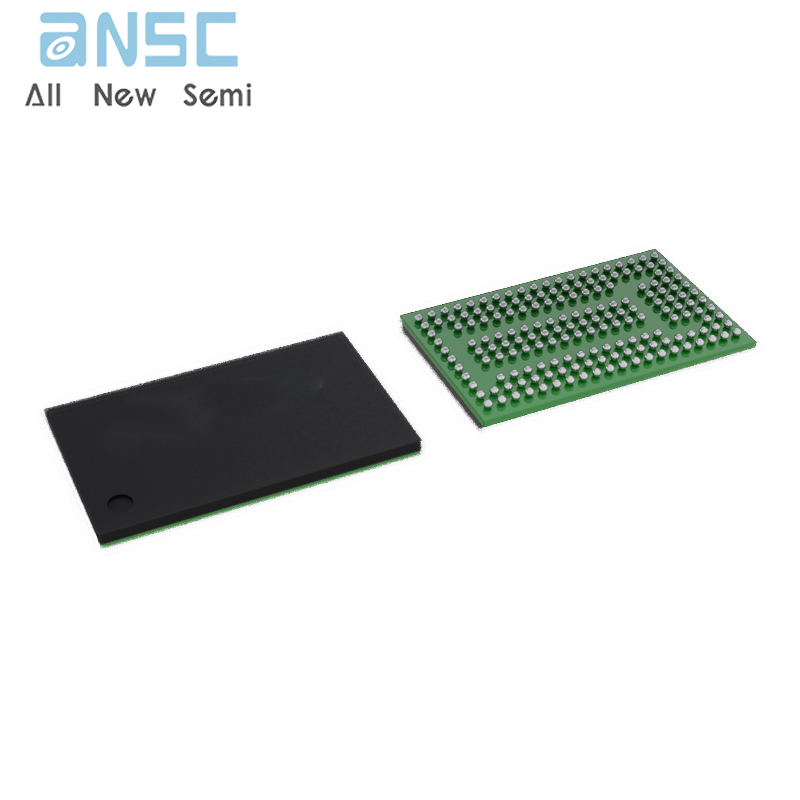
For more product information, please download the PDF
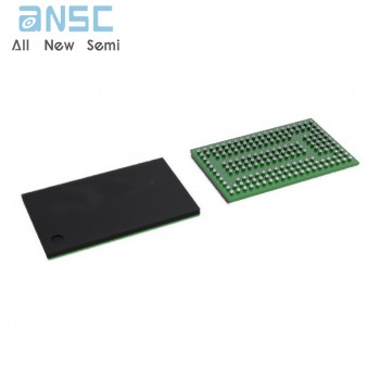
SSTE32882KB1AKG8 Pinout optimizes DDR3 RDIMM Clock Driver IC BGA spot stock
SEND
RFQ