+86 135 5637 6665
+852 2632 9637
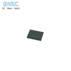
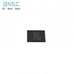
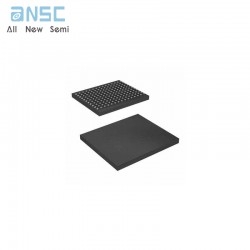
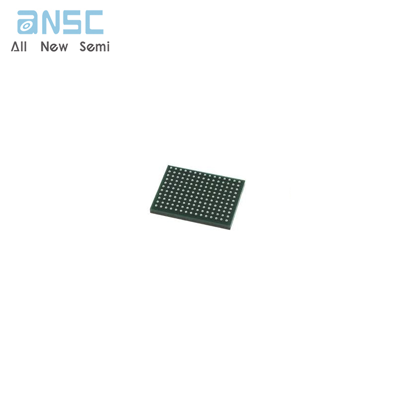
Image shown is a representation only.
Exact specifications should be obtained from the product data sheet.
CY7C1520KV18-250BZC SRAM - Synchronous, DDR II Memory IC 72Mbit Parallel 250 MHz 165-FBGA spot stock
The CY7C1518KV18, and CY7C1520KV18 are 1.8 Vsynchronous pipelined SRAM equipped with DDR II architecture .The DDR II consists of an SRAM core with advancedsynchronous peripheral circuitry and a 1-bit burst counter.Addresses for read and write are latched on alternate risingedges of the input (K)clock .Write data is registered on the risingedges of both K and K .Read data is driven on the rising edgesof C and C if provided,or on the rising edge of K and K if C/C arenot provided .On CY7C1518KV18 and CY7C1520KV18,theburst counter takes in the least significant bit of the externaladdress and bursts two 18-bit words in the case ofCY7C1518KV18 and two 36-bit words in the case ofCY7C1520KV18 sequentially into or out of the device .
Asynchronous inputs include an output impedance matchinginput (ZQ).Synchronous data outputs (Q,sharing the samephysical pins as the data inputs D)are tightly matched to the twooutput echo clocks CQ/CQ ,eliminating the need for separatelycapturing data from each individual DDR SRAM in the systemdesign .Output data clocks (C/C)enable maximum systemclocking and data synchronization flexibility.
All synchronous inputs pass through input registers controlled bythe K or K input clocks .All data outputs pass through outputregisters controlled by the C or C (or K or K in a single clockdomain) input clocks . Writes are conducted with on-chipsynchronous self-timed write circuitry.
■ 72-Mbit density (4M ×18,2M ×36)
■ 333 MHz clock for high bandwidth
■ Two-word burst for reducing address bus frequency
■ Double data rate (DDR) interfaces (data transferred at 666 MHz)at 333 MHz
■ Two input clocks (K and K)for precise DDR timing
❐ SRAM uses rising edges only
■ Two input clocks for output data (C and C)to minimize clock skew and flight time mismatches
■ Echo clocks (CQ and CQ)simplify data capture in high speed systems
■ Synchronous internally self-timed writes
■ DDR II operates with 1.5 cycle read latency when DOFF is asserted HIGH
■ Operates similar to DDR-I device with 1 cycle read latency when DOFF is asserted LOW
■ 1.8 V core power supply with HSTL inputs and outputs
■ Variable drive HSTL output buffers
■ Expanded HSTL output voltage (1.4 V–V DD)
❐ Supports both 1.5 V and 1.8 V IO supply
■ Available in 165-ball fine pitch ball grid array (FBGA)package (13 ×15 ×1.4 mm)
■ Offered in both Pb-free and non Pb-free packages
■ JTAG 1149.1 compatible Test Access Port
■ Phase-locked loop (PLL)for accurate data placement
| Attribute | Attribute value |
| ANSM-Part# | ANSM-CY7C1520KV18-250BZC |
| Category | Integrated Circuits (ICs) |
| Memory | |
| Memory | |
| Mfr | - |
| Packaging | Tray |
| Part Status | Active |
| DigiKey Programmable | Not Verified |
| Memory Type | Volatile |
| Memory Format | SRAM |
| Technology | SRAM - Synchronous, DDR II |
| Memory Size | 72Mbit |
| Memory Organization | 2M x 36 |
| Memory Interface | Parallel |
| Clock Frequency | 250 MHz |
| Voltage - Supply | 1.7V ~ 1.9V |
| Operating Temperature | 0°C ~ 70°C (TA) |
| Mounting Type | Surface Mount |
| Package / Case | 165-LBGA |
| Supplier Device Package | 165-FBGA (13x15) |
For more product information, please download the PDF
CY7C1520KV18-250BZC SRAM - Synchronous, DDR II Memory IC 72Mbit Parallel 250 MHz 165-FBGA spot stock
SEND
RFQ