
+86 135 5637 6665
+852 2632 9637


Image shown is a representation only.
Exact specifications should be obtained from the product data sheet.
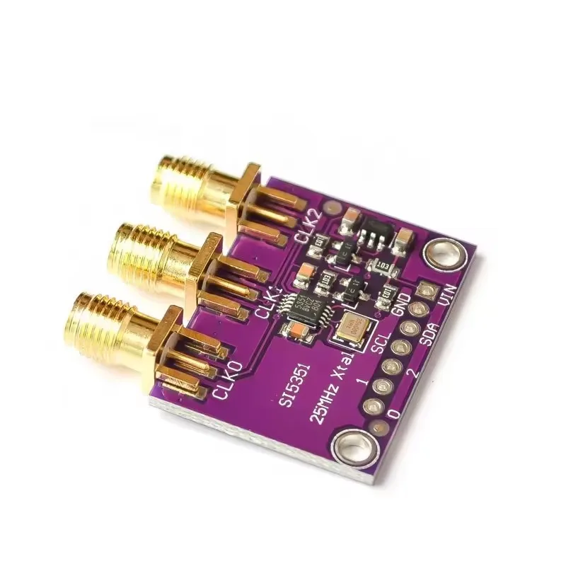
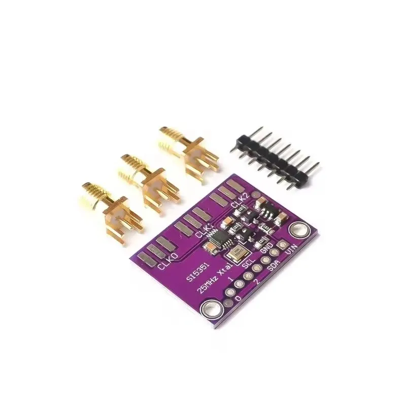
SI5351 High frequency signal square wave frequency generator Clock signal generator module signal generator
| Product Introduction The Si5351 is an I2C-configurable clock generator ideal for cost-sensitive applications replacing crystal oscillators, VCXOs, phase-locked loops (PLIs), and fanout buffers. Based on a PLL/VCO + high-resolution multi-synchronous fractional divider architecture, the Si5351 can generate any frequency up to 160 MHz with 0ppm error on each output. Three versions of the Si5351 address a wide range of applications. The Si5351A uses an internal oscillator designed to replace crystals and crystal oscillators. |
| Applications HDTV, DVD/Blu-ray, Set-Top Boxes Residential Gateways Audio/Video Equipment, Gaming Networking/Communications Printers, Scanners, Projectors Servers, Storage X0 Replacement |
| Product Features Generates up to 8 non-integer related frequencies from 8 kHz to 160 MHz User-definable I2C configuration Precise frequency synthesis (0 ppm error) on each output Highly linear VCX0 selectable clock input (CLKIN) Low output period jitter: 100 ps pp Optional configurable spread spectrum on each output Low-cost, fixed-frequency operation: 25 or 27 MHz Supports static phase offset Programmable rise/fall time control Glitch-free frequency variation Independent power supply pins: ①Core VDD: 2.5 V or 3.3 V ②Output VDDO: 1.8 V, 2.5 V, or 3.3 V Excellent PSRR eliminates external power supply filtering Very low power consumption Adjustable output-to-output delay Compliant with PCIe Gen 1 standards Supports HCSL-compliant swing Supply voltage: DC 3.3-5 V |
| Pin Functions SDA: Data pin SCL: Clock pin VIN: VCC GND: Ground Pin 0: Clock signal output channel 0 Pin 1: Clock signal output channel 1 |
Product Photos

Company Information
.jpg)
.jpg)
.jpg)
.jpg)

SI5351 High frequency signal square wave frequency generator Clock signal generator module signal generator
SEND
RFQ