+86 135 5637 6665
+852 2632 9637
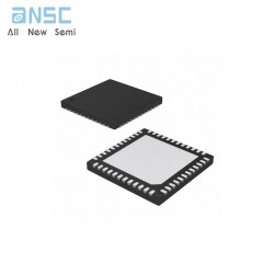
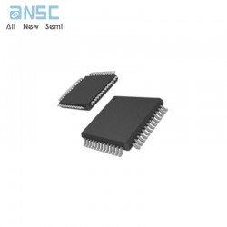
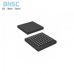
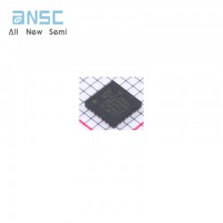
Image shown is a representation only.
Exact specifications should be obtained from the product data sheet.
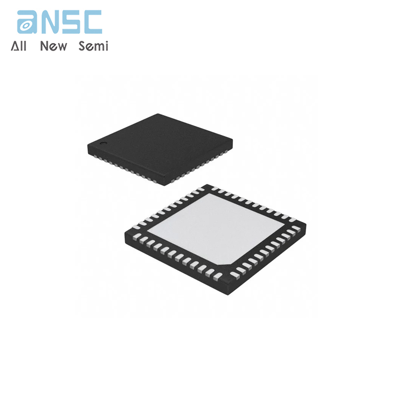
NB3M8T3910GMNR2G Configurable Differential Clock Fanout Buffer VFQF48 spot stock
The NB3M8T3910G is a 3:1:10 Clock fanout buffer operating on a2.5 V/3.3 V Core VDD and a flexible 2.5 V / 3.3 V VDDO supply(VDDO≤ V DD).
A 3:1 MUX selects between Crystal oscillator inputs, or either of two differential Clock inputs capable of accepting LVPECL, LVDS, HCSL, or SSTL levels. The MUX select lines, SEL0 and SEL1, accept LVCMOS or LVTTL levels and select input per Table 3. The Crystal input is disabled when a Clock input is selected.
Differential Outputs consist of two banks of five differential outputs with each bank independently mode configurable as LVPECL, LVDS or HCSL. Each bank of differential output pairs is configured with a pair of SMODEAx/Bx select lines using LVCMOS or LVTTL levels per Table 6. Clock input levels and outputs states are determined per Table 5.
The Single−Ended LVCMOS Output, REFOUT, is synchronously enabled by the OE_SE control line per Table 4 using LVCMOS / LVTTL levels. For Clock frequencies above 250 MHz, the REFOUTline should be disabled.
• Crystal, Single−Ended or Differential Input Reference Clocks
• Differential Input Pair can Accept: LVPECL, LVDS, HCSL, SSTL
• Two Output Banks: Each has Five Differential Outputs Configurable as LVPECL, LVDS, or HCSL by SMODEAx/Bx Pins
• One Single−Ended LVCMOS Output with Synchronous OE Control
• LVCMOS/LVTTL Interface Levels for all Control Inputs
• Clock Frequency: Up to 1400 MHz, Typical
• Output Skew: 50 ps (Max)
• Additive RMS Jitter <0.03 ps (156.25 MHz, Typical)
• Input to Output Propagation Delay (900 ps Typical)
• Operating Supply Modes V DD/VDDO: 2.5 V/2.5 V, 3.3 V/3 .3 V or 3.3 V/2 .5 V
• Industrial Temperature Range −40°C to 85°C
• This is a Pb−Free Device
• Clock Distribution
• Telecom
• Networking
• Backplane
• High End Computing
• Wireless and Wired Infrastructure
| Attribute | Attribute value |
| ANSM-Part# | ANSM-NB3M8T3910GMNR2G |
| Category | Integrated Circuits (ICs) |
| Clock/Timing | |
| Clock Buffers, Drivers | |
| Manufacturer | - |
| Packaging | Tape & Reel (TR) |
| Part Status | Obsolete |
| Type | Fanout Buffer (Distribution), Multiplexer |
| Number of Circuits | 1 |
| Ratio - Input:Output | 3:10 |
| Differential - Input:Output | Yes/Yes |
| Input | HCSL, LVDS, LVPECL, SSTL, Crystal |
| Output | HCSL, LVCMOS, LVDS, LVPECL |
| Frequency - Max | 1.4 GHz |
| Voltage - Supply | 2.375V ~ 3.465V |
| Operating Temperature | -40°C ~ 85°C |
| Mounting Type | Surface Mount |
| Package / Case | 48-VFQFN Exposed Pad |
| Supplier Device Package | 48-QFN (7x7) |
| Base Product Number | NB3M8 |
For more product information, please download the PDF
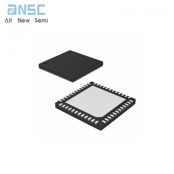
NB3M8T3910GMNR2G Configurable Differential Clock Fanout Buffer VFQF48 spot stock
SEND
RFQ