+86 135 5637 6665
+852 2632 9637
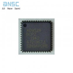
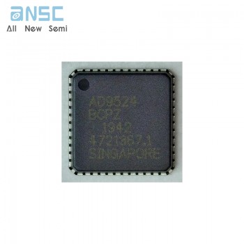
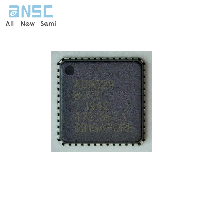
Image shown is a representation only.
Exact specifications should be obtained from the product data sheet.
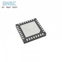
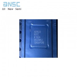
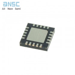
AD9524BCPZ Jitter Cleaner and Clock Generator 48VFQFN spot stock
The AD9524 provides a low power, multi-output, clock distributionfunction with low jitter performance, along with an on-chip PLL andVCO . The on-chip VCO tunes from 3.6 GHz to 4.0 GHz .
The AD9524 is defined to support the clock requirements for longterm evolution (LTE) and multicarrier GSM base station designs . Itrelies on an external VCXO to provide the reference jitter cleanup toachieve the restrictive low phase noise requirements necessary foracceptable data converter SNR performance .
The input receivers, oscillator, and zero delay receiver provide bothsingle-ended and differential operation . When connected to a recovered system reference clock and a VCXO, the device generatessix low noise outputs with a range of 1 MHz to 1 GHz, and onededicated buffered output from the input PLL (PLL1). The frequencyand phase of one clock output relative to another clock output canbe varied by means of a divider phase select function that servesas a jitter-free coarse timing adjustment in increments that areequal to one-half the period of the signal coming out of the VCO .
An in-package EEPROM can be programmed through the serialinterface to store user defined register settings for power-up andchip reset .
► Output frequency: <1 MHz to 1 GHz
► Start-up frequency accuracy: <±100 ppm (determined by VCXO reference accuracy)
► Zero delay operation
► Input-to-output edge timing: <±150 ps
► 6 outputs: configurable LVPECL, LVDS, HSTL, and LVCMOS
► 6 dedicated output dividers with jitter-free adjustable delay
► Adjustable delay: 63 resolution steps of ½ period of VCO output divider
► Output-to-output skew: <±50 ps
► Duty-cycle correction for odd divider settings
► Automatic synchronization of all outputs on power-up
► Absolute output jitter: <200 fs at 122.88 MHz
► Integration range: 12 kHz to 20 MHz
► Distribution phase noise floor: −160 dBc/Hz
► Digital lock detect
► Nonvolatile EEPROM stores configuration settings
► SPI- and I2 C-compatible serial control port
► Dual PLL architecture
► PLL1
► Low bandwidth for reference input clock cleanup with external VCXO
► Phase detector rate up to 130 MHz
► Redundant reference inputs
► Automatic and manual reference switchover modes
► Revertive and nonrevertive switching
► Loss of reference detection with holdover mode
► Low noise LVCMOS output from VCXO used for RF/IF synthesizers
► PLL2
► Phase detector rate of up to 259 MHz
► Integrated low noise VCO
► LTE and multicarrier GSM base stations
► Wireless and broadband infrastructure
► Medical instrumentation
► Clocking high speed ADCs, DACs, DDSs, DDCs, DUCs, MxFEs
► Low jitter, low phase noise clock distribution
► Clock generation and translation for SONET, 10Ge, 10G FC, and other 10 Gbps protocols
► Forward error correction (G .710)
► High performance wireless transceivers
| Attribute | Attribute value |
| ANSM-Part# | ANSM-AD9524BCPZ |
| Category | Integrated Circuits (ICs) |
| Clock/Timing | |
| Application Specific Clock/Timing | |
| Manufacturer | - |
| Packaging | Tray |
| Part Status | Active |
| DigiKey Programmable | Not Verified |
| PLL | Yes |
| Main Purpose | Ethernet, Fibre Channel, SONET/SDH |
| Input | CMOS |
| Output | HSTL, LVCMOS, LVDS, LVPECL |
| Number of Circuits | 1 |
| Ratio - Input:Output | 2:6 |
| Differential - Input:Output | Yes/Yes |
| Frequency - Max | 1GHz |
| Voltage - Supply | 1.71V ~ 3.465V |
| Operating Temperature | -40°C ~ 85°C |
| Mounting Type | Surface Mount |
| Package / Case | 48-VFQFN Exposed Pad, CSP |
| Supplier Device Package | 48-LFCSP-VQ (7x7) |
| Base Product Number | AD9524 |
For more product information, please download the PDF
AD9524BCPZ Jitter Cleaner and Clock Generator 48VFQFN spot stock
SEND
RFQ