Clock/Timer ICs
High Demand, Limited Stock MT48LC1M16A1TG-6S TSOP offer BOM services spot stock
$0.00
+86 135 5637 6665
+852 2632 9637

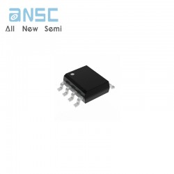
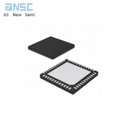
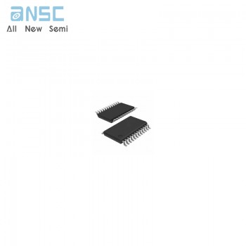
Image shown is a representation only.
Exact specifications should be obtained from the product data sheet.
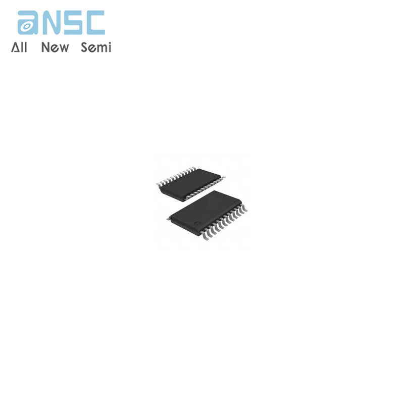
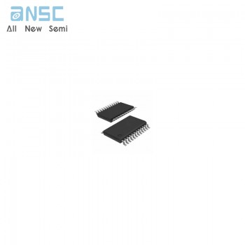
CDCVF2509APW 3.3-V PHASE-LOCK LOOP CLOCK DRIVER IC
The CDCVF2509A is a high-performance, low-skew, low-jitter, phase-lock loop (PLL) clock driver . It uses a PLL to precisely align, in both frequency and phase, the feedback (FBOUT) output to the clock (CLK) input signal . It is specifically designed for use with synchronous DRAMs . The CDCVF2509A operates at a 3.3-V VCC . It also provides integrated series-damping resistors that make it ideal for driving point-to-point loads .
One bank of five outputs and one bank of four outputs provide nine low-skew, low-jitter copies of CLK . Output signal duty cycles are adjusted to 50%, independent of the duty cycle at CLK . Each bank of outputs is enabled or disabled separately via the control (1G and 2G) inputs . When the G inputs are high, the outputs switch in phase and frequency with CLK; when the G inputs are low, the outputs are disabled to the logic-low state . The deviceautomically goes into power-down mode when no input signal (< 1 MHz) is applied to CLK; the outputs go into a low state .
• Designed to Meet and Exceed PC133 SDRAM Registered DIMM Specification Rev . 1.1
• Spread Spectrum Clock Compatible
• Operating Frequency 20 MHz to 175 MHz
• Static Phase Error Distribution at 66 MHz to 166 MHz Is ±125 ps
• Jitter (cyc - cyc) at 66 MHz to 166 MHz Is |70| ps
• Advanced Deep Submicron ProcessResults in More Than 40% Lower Power Consumption Versus Current Generation PC133 Devices
• Auto Frequency Detection to Disable Device (Power-Down Mode)
• Available in Plastic 24-Pin TSSOP
• Phase-Lock Loop Clock Distribution for Synchronous DRAM Applications
• Distributes One Clock Input to One Bank of Five and One Bank of Four Outputs
• Separate Output Enable for Each Output Bank
• External Feedback (FBIN) Terminal Is Used to Synchronize the Outputs to the Clock Input
• 25-Ω On-Chip Series Damping Resistors
• No External RC Network Required
• Operates at 3.3 V
• DRAM Applications
• PLL Based Clock Distributors
• Non-PLL Clock Buffer
| Attribute | Attribute value |
| ANSM-Part# | ANSM-CDCVF2509APW |
| Category | Integrated Circuits (ICs) |
| Clock/Timing | |
| Clock Generators, PLLs, Frequency Synthesizers | |
| Manufacturer | - |
| Packaging | Tube |
| Part Status | Obsolete |
| DigiKey Programmable | Not Verified |
| Type | PLL Clock Driver |
| PLL | Yes with Bypass |
| Input | LVTTL |
| Output | LVTTL |
| Number of Circuits | 1 |
| Ratio - Input:Output | 2:10 |
| Differential - Input:Output | No/No |
| Frequency - Max | 175MHz |
| Divider/Multiplier | No/No |
| Voltage - Supply | 3V ~ 3.6V |
| Operating Temperature | 0°C ~ 85°C |
| Mounting Type | Surface Mount |
| Package / Case | 24-TSSOP (0.173", 4.40mm Width) |
| Supplier Device Package | 24-TSSOP |
| Base Product Number | CDCVF2509 |
For more product information, please download the PDF
CDCVF2509APW 3.3-V PHASE-LOCK LOOP CLOCK DRIVER IC
SEND
RFQ