+86 135 5637 6665
+852 2632 9637
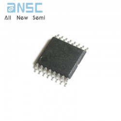
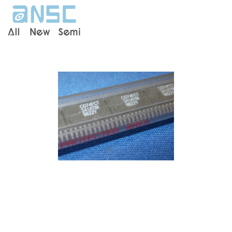
Image shown is a representation only.
Exact specifications should be obtained from the product data sheet.
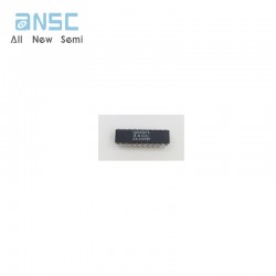
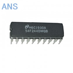
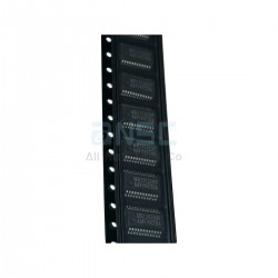
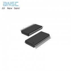
CD74FCT241TM FCT Interface Logic Octal Buffers/Line Drivers, Three-State SOP spot stock
The CD54/74FCT240, 240AT, 241, 244 and 244AT threestate octal buffers/line drivers use a small-geometry BiCMOS technology. The output stage is a combination of bipolar and CMOS transistors that limits the output-HIGH level to two diode drops below VCC. This resultant lowering of output swing (0V to 3.7V) reduces power bus ringing (a source of EMI) and minimizes VCC bounce and ground bounce and their effects during simultaneous output switching. The output configuration also enhances switching speed and is capable of sinking 48mA to 64mA.
The CD54/74FCT240, 240AT, 244 and 244AT have activeLOW output enables (1OE, 2OE). The CD54/74FCT241 and CD54/74FCT241AT have one active-LOW (1OE) and one active-HIGH (2OE) output enable.
• CD54/74FCT240, CD54/74FCT240AT - Inverting
• CD54/74FCT241, CD54/74FCT244, CD54/74FCT244AT - Non-Inverting
• Buffered Inputs
• Typical Propagation Delay: 4.1ns at VCC = 5V, TA = 25oC (FCT240AT, FCT244AT)
• SCR-Latchup-Resistant BiCMOS Process and Circuit Design
• FCTXXX Types - Speed of Bipolar FAST®/AS/S; FCTXXXAT Types - 30% Faster Than FAST/AS/S with Significantly Reduced Power Consumption
• 48mA to 64mA Output Sink Current (Commer cial/Extended Industrial)
• Output Voltage Swing Limited to 3.7V at VCC = 5V
• Controlled Output-Edge Rates
• Input/Output Isolation to VCC
• BiCMOS Technology with Low Quiescent Power
For more product information, please download the PDF
CD74FCT241TM FCT Interface Logic Octal Buffers/Line Drivers, Three-State SOP spot stock
SEND
RFQ