+86 135 5637 6665
+852 2632 9637
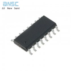
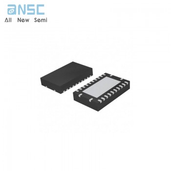
Image shown is a representation only.
Exact specifications should be obtained from the product data sheet.
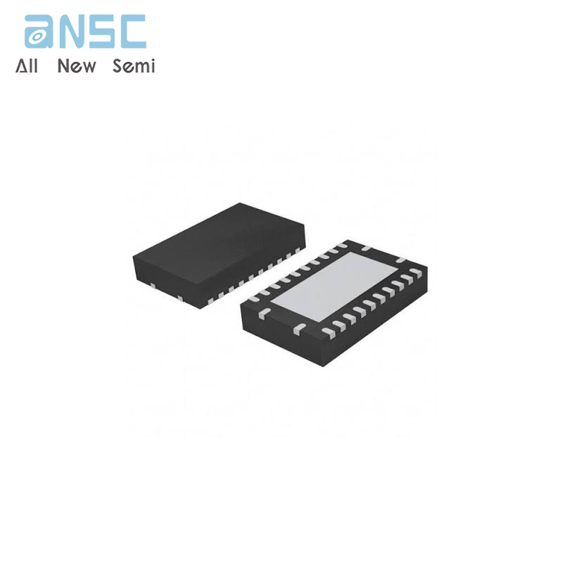
74LVCH8T245BQ,118 8-bit dual supply translating transceiver IC QFN spot stock
The 74LVC8T245; 74LVCH8T245 are 8-bit dual supply translating transceivers with 3-state outputsthat enable bidirectional level translation . They feature two data input-output ports (pins An andBn), a direction control input (DIR), an output enable input (OE) and dual supply pins (V CC(A) andV CC(B)). Both V CC(A) and V CC(B) can be supplied at any voltage between 1.2 V and 5.5 V makingthe device suitable for translating between any of the low voltage nodes (1 .2 V, 1.5 V, 1.8 V, 2.5 V,3.3 V and 5.0 V). Pins An, OE and DIR are referenced to V CC(A) and pins Bn are referenced toV CC(B). A HIGH on DIR allows transmission from An to Bn and a LOW on DIR allows transmissionfrom Bn to An . The output enable input (OE) can be used to disable the outputs so the buses areeffectively isolated .
The devices are fully specified for partial power-down applications using I OFF . The I OFF circuitrydisables the output, preventing any damaging backflow current through the device when it ispowered down . In suspend mode when either V CC(A) or V CC(B) are at GND level, both A port andB port are in the high-impedance OFF-state
Active bus hold circuitry in the 74LVCH8T245 holds unused or floating data inputs at a valid logiclevel .
• Wide supply voltage range:
• V CC(A): 1.2 V to 5.5 V
• V CC(B): 1.2 V to 5.5 V
• High noise immunity
• Complies with JEDEC standards:
• JESD8-7 (1 .2 V to 1.95 V)
• JESD8-5 (1 .8 V to 2.7 V)
• JESD8C (2 .7 V to 3.6 V)
• JESD36 (4 .5 V to 5.5 V)
• Maximum data rates:
• 420 Mbps (3 .3 V to 5.0 V translation)
• 210 Mbps (translate to 3.3 V)
• 140 Mbps (translate to 2.5 V)
• 75 Mbps (translate to 1.8 V)
• 60 Mbps (translate to 1.5 V)
• Suspend mode
• Latch-up performance exceeds 100 mA per JESD 78B Class II
• ±24 mA output drive (VCC = 3.0 V)
• Inputs accept voltages up to 5.5 V
• Low power consumption: 30 μA maximum I CC
• I OFF circuitry provides partial Power-down mode operation
• ESD protection:
• HBM: ANSI/ESDA/JEDEC JS-001 class 3A exceeds 4000 V
• CDM: ANSI/ESDA/JEDEC JS-002 class C3 exceeds 1000 V
• Specified from -40 °C to +85 °C and -40 °C to +125 °C
| Attribute | Attribute value |
| ANSM-Part# | ANSM-74LVCH8T245BQ,118 |
| Category | Integrated Circuits (ICs) |
| Logic | |
| Buffers, Drivers, Receivers, Transceivers | |
| Manufacturer | - |
| Series | 74LVCH |
| Packaging | Tape & Reel (TR) |
| Cut Tape (CT) | |
| Digi-Reel® | |
| Part Status | Active |
| Logic Type | Translation Transceiver |
| Number of Elements | 1 |
| Number of Bits per Element | 8 |
| Output Type | 3-State |
| Current - Output High, Low | 32mA, 32mA |
| Voltage - Supply | 1.2V ~ 5.5V |
| Operating Temperature | -40°C ~ 125°C (TA) |
| Mounting Type | Surface Mount |
| Package / Case | 24-VFQFN Exposed Pad |
| Supplier Device Package | 24-DHVQFN (5.5x3.5) |
| Base Product Number | 74LVCH8T245 |
For more product information, please download the PDF
74LVCH8T245BQ,118 8-bit dual supply translating transceiver IC QFN spot stock
SEND
RFQ