
+86 135 5637 6665
+852 2632 9637
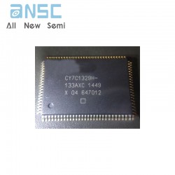
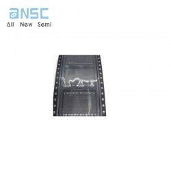
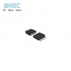
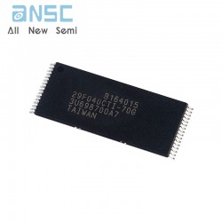
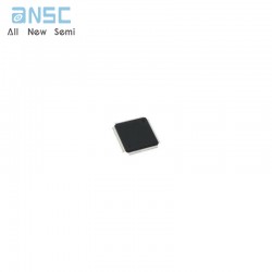
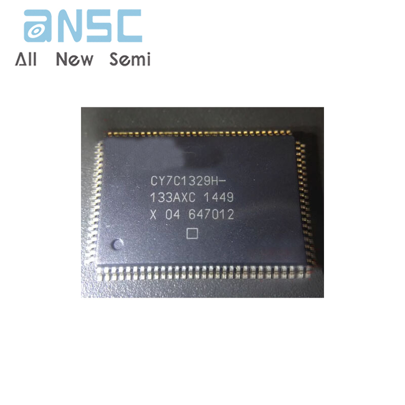
Image shown is a representation only.
Exact specifications should be obtained from the product data sheet.
CY7C1329H-133AXC 2-Mbit (64 K x 32) Pipelined Sync SRAM 2.5 V/3.3 V I/O operation QFP
The CY7C1329H[1] SRAM integrates 64 K × 32 SRAM cells with advanced synchronous peripheral circuitry and a two-bit counter for internal burst operation. All synchronous inputs are gated by registers controlled by a positive-edge-triggered Clock Input (CLK). The synchronous inputs include all addresses, all data inputs, address-pipelining Chip Enable (CE1), depth-expansion Chip Enables (CE2 and CE3), Burst Control inputs (ADSC, ADSP, and ADV), Write Enables (BW[A:D] and BWE), and Global Write (GW). Asynchronous inputs include the Output Enable (OE) and the ZZ pin.
Addresses and chip enables are registered at rising edge of clock when either Address Strobe Processor (ADSP) or Address Strobe Controller (ADSC) are active. Subsequent burst addresses can be internally generated as controlled by the Advance pin (ADV).
Address, data inputs, and write controls are registered on-chip to initiate a self-timed Write cycle. This part supports Byte Write operations (see Pin Descriptions and Truth Table for further details). Write cycles can be one to four bytes wide as controlled by the Byte Write control inputs. GW when active LOW causes all bytes to be written.
The CY7C1329H operates from a +3.3 V core power supply while all outputs operate with either a +2.5 V or +3.3 V supply. All inputs and outputs are JEDEC-standard JESD8-5-compatible.
■ Registered inputs and outputs for pipelined operation
■ 64 K × 32 common I/O architecture
■ 3.3 V core power supply
■ 2.5 V/3.3 V I/O operation
■ Fast clock-to-output times
❐ 3.5 ns (for 166-MHz device)
❐ 4.0 ns (for 133-MHz device)
■ Provide high-performance 3-1-1-1 access rate
■ User-selectable burst counter supporting Intel Pentium® interleaved or linear burst sequences
■ Separate processor and controller address strobes
■ Synchronous self-timed write
■ Asynchronous output enable
■ Offered in JEDEC-standard lead-free 100-pin TQFP package
■ “ZZ” Sleep Mode Option
| Attribute | Attribute value |
| ANSM-Part# | ANSM-CY7C1329H-133AXC |
| Category | Integrated Circuits (ICs) |
| Memory | |
| Memory | |
| Mfr | - |
| Series | - |
| Packaging | Tray |
| Part Status | Obsolete |
| DigiKey Programmable | Not Verified |
| Memory Type | Volatile |
| Memory Format | SRAM |
| Technology | SRAM - Synchronous, SDR |
| Memory Size | 2Mbit |
| Memory Organization | 64K x 32 |
| Memory Interface | Parallel |
| Clock Frequency | 133 MHz |
| Write Cycle Time - Word, Page | - |
| Access Time | 4 ns |
| Voltage - Supply | 3.15V ~ 3.6V |
| Operating Temperature | 0°C ~ 70°C (TA) |
| Mounting Type | Surface Mount |
| Package / Case | 100-LQFP |
| Supplier Device Package | 100-TQFP (14x20) |
| Base Product Number | CY7C1329 |
For more product information, please download the PDF
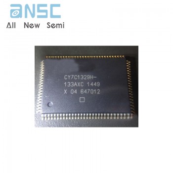
CY7C1329H-133AXC 2-Mbit (64 K x 32) Pipelined Sync SRAM 2.5 V/3.3 V I/O operation QFP
SEND
RFQ