+86 135 5637 6665
+852 2632 9637
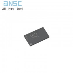
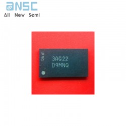
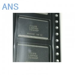
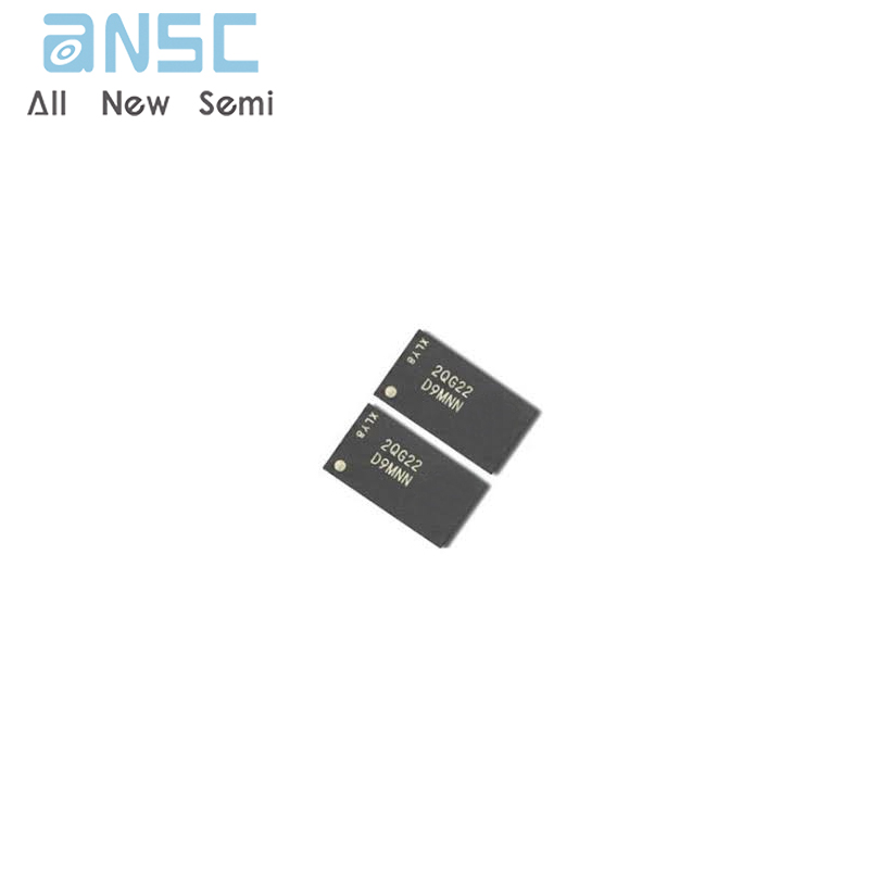
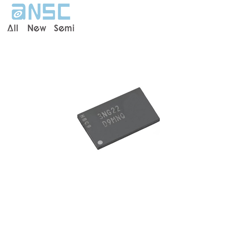
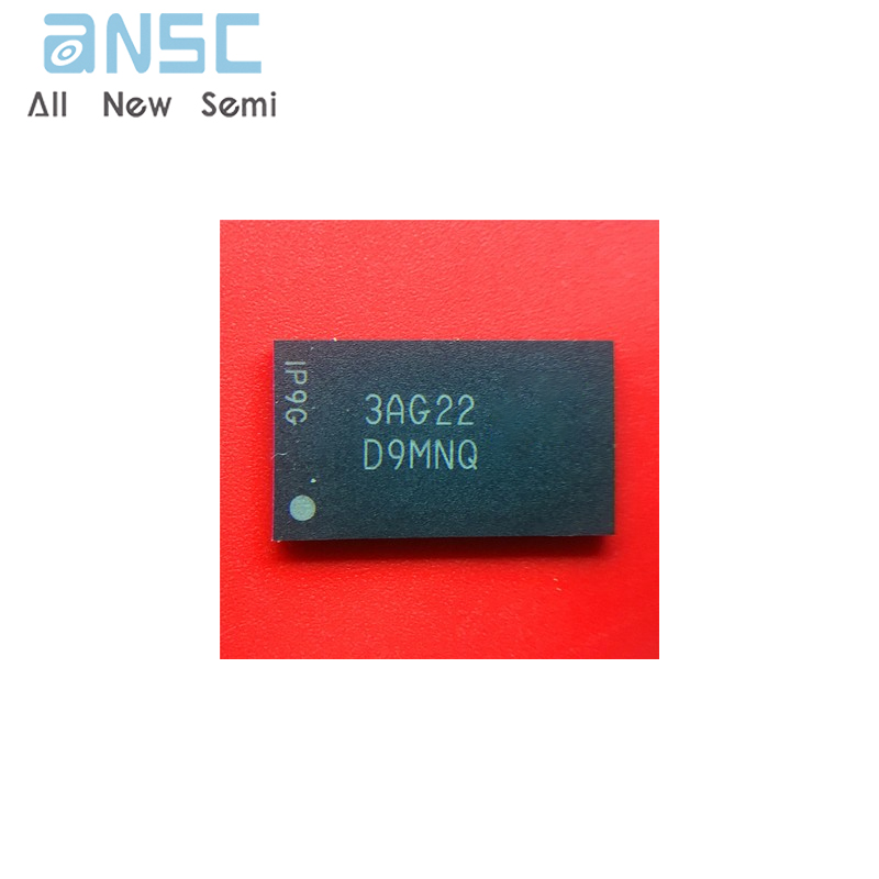
Image shown is a representation only.
Exact specifications should be obtained from the product data sheet.
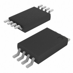
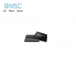
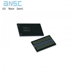
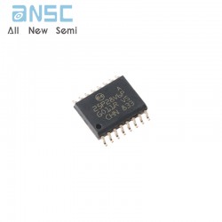
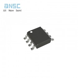
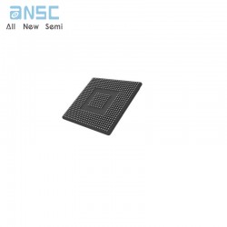
MT41J64M16JT-125:G SDRAM - DDR3 Memory IC 1Gbit Parallel 800 MHz 96-FBGA
The DDR3 SDRAM uses a double data rate architecture to achieve high-speed operation. The double data rate architecture is an 8n-prefetch architecture with an interface designed to transfer two data words per clock cycle at the I/O pins. A single read or write access for the DDR3 SDRAM consists of a single 8n-bit-wide, one-clock-cycle data transfer at the internal DRAM core and eight corresponding n-bit-wide, one-half-clockcycle data transfers at the I/O pins.
The differential data strobe (DQS, DQS#) is transmitted externally, along with data, for use in data capture at the DDR3 SDRAM input receiver. DQS is center-aligned with data for WRITEs. The read data is transmitted by the DDR3 SDRAM and edge-aligned to the data strobes.
The DDR3 SDRAM operates from a differential clock (CK and CK#). The crossing of CK going HIGH and CK# going LOW is referred to as the positive edge of CK. Control, command, and address signals are registered at every positive edge of CK. Input data is registered on the first rising edge of DQS after the WRITE preamble, and output data is referenced on the first rising edge of DQS after the READ preamble.
• VDD = VDDQ = +1.5V ±0.075V
• 1.5V center-terminated push/pull I/O
• Differential bidirectional data strobe
• 8n-bit prefetch architecture
• Differential clock inputs (CK, CK#)
• 8 internal banks
• Nominal and dynamic on-die termination (ODT) for data, strobe, and mask signals
• CAS (READ) latency (CL): 5, 6, 7, 8, 9, 10, or 11
• POSTED CAS ADDITIVE latency (AL): 0, CL - 1, CL - 2
• CAS (WRITE) latency (CWL): 5, 6, 7, 8, based on tCK
• Fixed burst length (BL) of 8 and burst chop (BC) of 4 (via the mode register set [MRS])
• Selectable BC4 or BL8 on-the-fly (OTF)
• Self refresh mode
• TC of 0oC to 95oC
– 64ms, 8,192 cycle refresh at 0oC to 85oC
– 32ms at 85oC to 95oC
• Clock frequency range of 300–800 MHz
• Self refresh temperature (SRT)
• Automatic self refresh (ASR)
• Write leveling
• Multipurpose register
• Output driver calibration
For more product information, please download the PDF

MT41J64M16JT-125:G SDRAM - DDR3 Memory IC 1Gbit Parallel 800 MHz 96-FBGA
SEND
RFQ