+86 135 5637 6665
+852 2632 9637
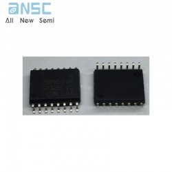
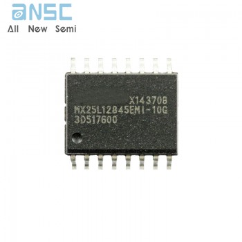
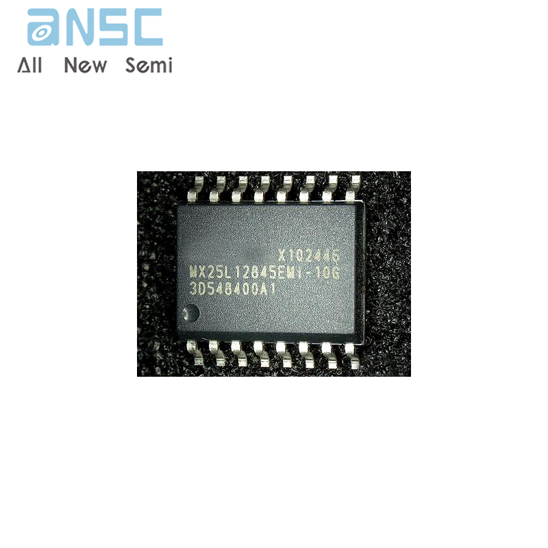
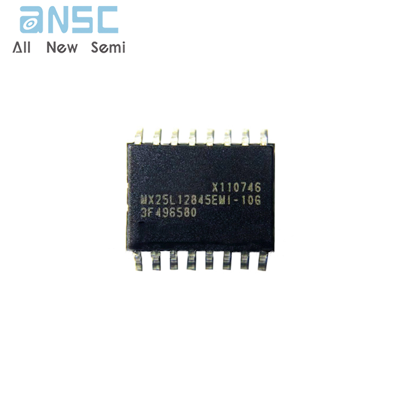
Image shown is a representation only.
Exact specifications should be obtained from the product data sheet.
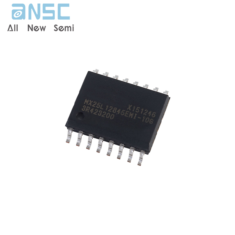
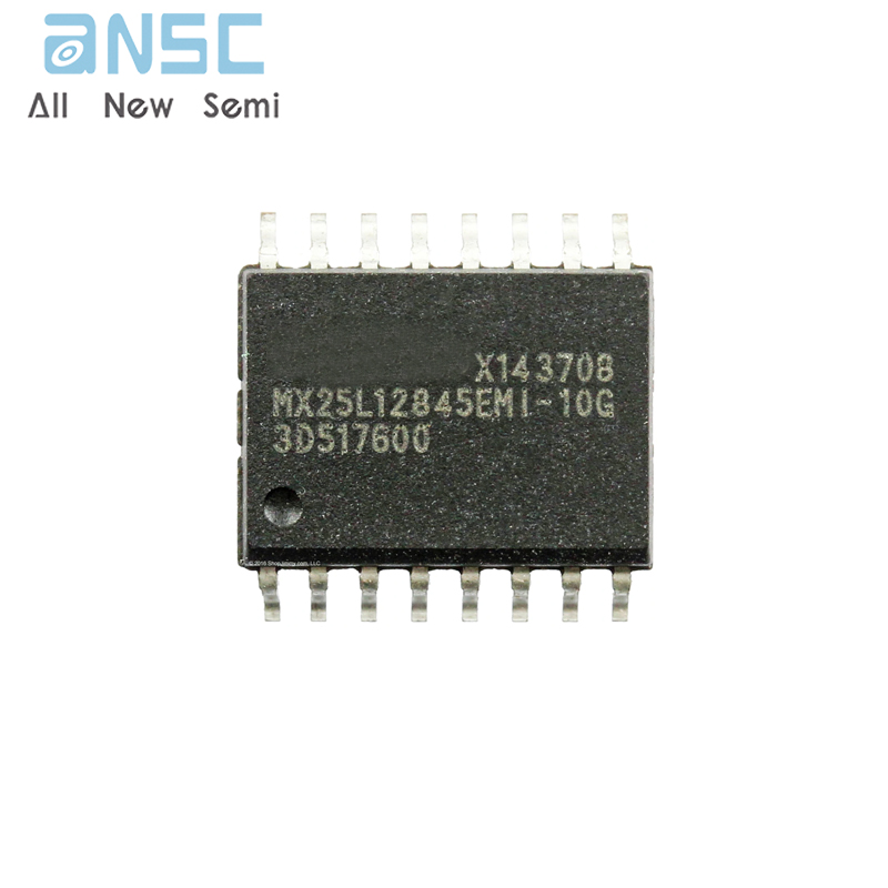
MX25L12845EMI-10G 128M-BIT CMOS MXSMIO FLASH MEMORY SOP16
MX25L12845E is 134,217,728 bits serial Flash memory, which is configured as 16,777,216 x 8 internally. When it is in two or four I/O mode, the structure becomes 67,108,864 bits x 2 or 33,554,432 bits x 4. The MX25L12845E features a serial peripheral interface and software protocol allowing operation on a simple 3-wire bus. The three bus signals are a clock input (SCLK), a serial data input (SI), and a serial data output (SO). Serial access to the device is enabled by CS# input.
MX25L12845E provides high performance read mode, which may latch address and data on both rising and falling edge of clock. By using this high performance read mode, the data throughput may be doubling. Moreover, the performance may reach direct code execution, the RAM size of the system may be reduced and further saving system cost.
MX25L12845E, MXSMIO (Serial Multi I/O) flash memory, provides sequential read operation on the whole chip and multi-I/O features.
When it is in dual I/O mode, the SI pin and SO pin become SIO0 pin and SIO1 pin for address/dummy bits input and data output. When it is in quad I/O mode, the SI pin, SO pin, WP# pin and NC pin become SIO0 pin, SIO1 pin, SIO2 pin and SIO3 pin for address/dummy bits input and data Input/Output. Parallel mode is also provided in this device. It features 8 bit input/output for increasing throughputs. This feature is recommeded to be used for factory production purpose.
After program/erase command is issued, auto program/erase algorithms which program/erase and verify the specified page or sector/block locations will be executed. Program command is executed on byte basis, or page (256 bytes) basis, or word basis. Continuously Program mode and erase command are executed on 4K-byte sector, 32Kbyte/64K-byte block, or whole chip basis.
• Serial Peripheral Interface compatible -- Mode 0 and Mode 3
• 128Mb: 134,217,728 x 1 bit structure or 67,108,864 x 2 bits (two I/O mode) structure or 33,554,432 x 4 bits (four I/O mode) structure
• 4096 Equal Sectors with 4K bytes each
- Any Sector can be erased individually
• 512 Equal Blocks with 32K bytes each
- Any Block can be erased individually
• 256 Equal Blocks with 64K bytes each
- Any Block can be erased individually
• Power Supply Operation
- 2.7 to 3.6 volt for read, erase, and program operations
• Latch-up protected to 100mA from -1V to Vcc +1V
| Attribute | Attribute value |
| ANSM-Part# | ANSM-MX25L12845EMI-10G |
| Category | Integrated Circuits (ICs) |
| Memory | |
| Memory | |
| Mfr | - |
| Series | MX25xxx45 - MXSMIO™ |
| Packaging | Tube |
| Part Status | Not For New Designs |
| DigiKey Programmable | Not Verified |
| Memory Type | Non-Volatile |
| Memory Format | FLASH |
| Technology | FLASH - NOR |
| Memory Size | 128Mbit |
| Memory Organization | 16M x 8 |
| Memory Interface | SPI |
| Clock Frequency | 104 MHz |
| Write Cycle Time - Word, Page | 300µs, 5ms |
| Voltage - Supply | 2.7V ~ 3.6V |
| Operating Temperature | -40°C ~ 85°C (TA) |
| Mounting Type | Surface Mount |
| Package / Case | 16-SOIC (0.295", 7.50mm Width) |
| Supplier Device Package | 16-SOP |
| Base Product Number | MX25L12845 |
For more product information, please download the PDF
MX25L12845EMI-10G 128M-BIT CMOS MXSMIO FLASH MEMORY SOP16
SEND
RFQ