+86 135 5637 6665
+852 2632 9637
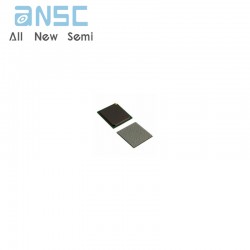
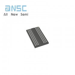
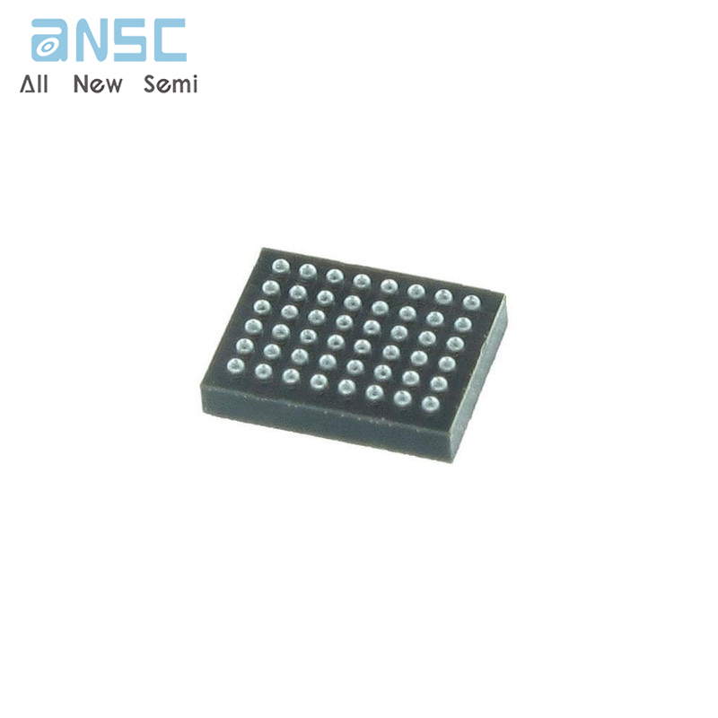
Image shown is a representation only.
Exact specifications should be obtained from the product data sheet.
CY62167DV30LL-70BVI 16-Mbit (1 M × 16) Static RAM BGA spot stock
The CY62167DV30 is a high-performance CMOS static RAM organized as 1M words by 16-bits. This device features advanced circuit design to provide ultra-low active current. This is ideal for providing More Battery Life(MoBL) in portable applications such as cellular telephones.The device also has an automatic power-down feature that significantly reduces power consumption by 99% when addresses are not toggling. The device can also be put into standby mode when deselected (CE 1 HIGH or CE 2 LOW or both BHE and BLE are HIGH). The input/output pins (I/O 0 through I/O 15) are placed in a high-impedance state when: deselected (CE 1 HIGH or CE 2 LOW), outputs are disabled (OE HIGH), both Byte High Enable and Byte Low Enable are disabled (BHE , BLE HIGH), or during a Write operation (CE 1 LOW, CE 2 HIGH and WE LOW).
Writing to the device is accomplished by taking Chip Enables(CE 1 LOW and CE2 HIGH) and Write Enable (WE) input LOW. If Byte Low Enable (BLE) is LOW, then data from I/O pins (I/O 0 through I/O 7),is written into the location specified on the address pins (A 0 through A 19). If Byte High Enable (BHE) is LOW, then data from I/O pins (I/O 8 through I/O 15) is written into the location specified on the address pins (A 0through A 19).
Reading from the device is accomplished by taking Chip Enables(CE 1 LOW and CE 2 HIGH) and Output Enable (OE) LOW while forcing the Write Enable (WE) HIGH. If Byte Low Enable (BLE) is LOW, then data from the memory location specified by the address pins appear on I/O 0 to I/O 7 . If Byte High Enable (BHE) is LOW,then data from memory appear on I/O 8to I/O 15 . See the truth table at the back of this data sheet for a complete description of Read and Write modes.
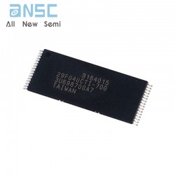
■ Thin small outline package (TSOP-I) configurable as
1 M × 16 or as 2 M × 8 SRAM
■ Wide voltage range: 2.2 V–3 .6 V
■ Ultra-low active power:
Typical active current: 2 mA at f = 1 MHz
■ Ultra-low standby power
■ Easy memory expansion with CE 1 , CE 2 and OE features
■ Automatic power-down when deselected
■ Complementary metal oxide semiconductor (CMOS) for optimum speed / power
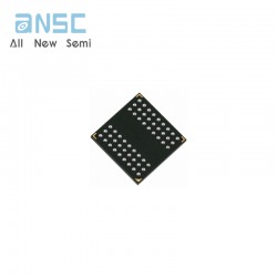
■ Available in Pb-free and non Pb-free 48-ball very fine-pitch ball grid array (VFBGA) and 48-pin TSOP I package
| Attribute | Attribute value |
| ANSM-Part# | ANSM-CY62167DV30LL-70BVI |
| Category | Integrated Circuits (ICs) |
| Memory | |
| Memory | |
| Mfr | - |
| Series | MOBL™ |
| Packaging | Tray |
| Part Status | Obsolete |
| DigiKey Programmable | Not Verified |
| Memory Type | Volatile |
| Memory Format | SRAM |
| Technology | SRAM - Asynchronous |
| Memory Size | 16Mbit |
| Memory Organization | 2M x 8, 1M x 16 |
| Memory Interface | Parallel |
| Write Cycle Time - Word, Page | 70ns |
| Access Time | 70 ns |
| Voltage - Supply | 2.2V ~ 3.6V |
| Operating Temperature | -40°C ~ 85°C (TA) |
| Mounting Type | Surface Mount |
| Package / Case | 48-VFBGA |
| Supplier Device Package | 48-VFBGA (8x9.5) |
| Base Product Number | CY62167 |
For more product information, please download the PDF
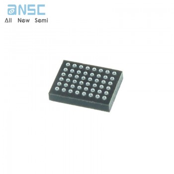
CY62167DV30LL-70BVI 16-Mbit (1 M × 16) Static RAM BGA spot stock
SEND
RFQ