+86 135 5637 6665
+852 2632 9637
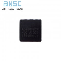
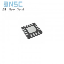
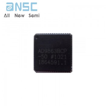
Image shown is a representation only.
Exact specifications should be obtained from the product data sheet.
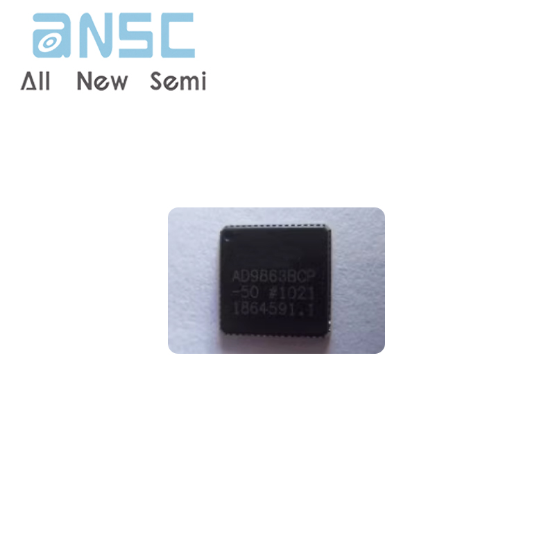
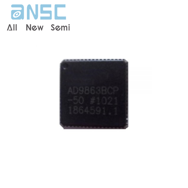
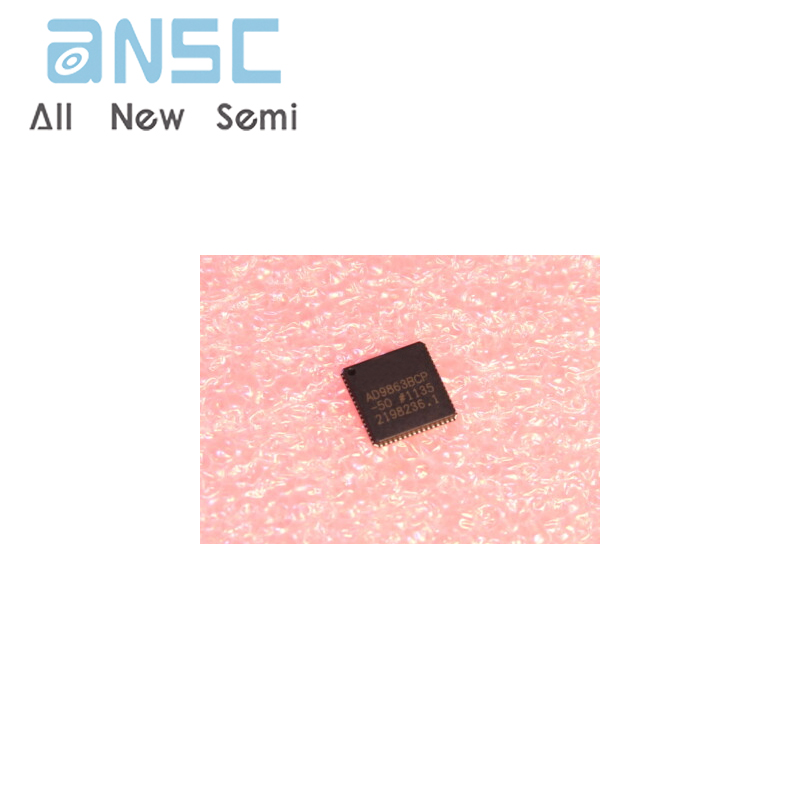
AD9863BCPZ-50 Transceiver for Broadband Applications QFN
The AD9863 is a member of the MxFE family—a group of integrated converters for the communications market. The AD9863 integrates dual 12-bit analog-to-digital converters (ADC) and dual 12-bit digital-to-analog converters (TxDAC®). The AD9863 ADCs are optimized for ADC sampling of 50 MSPS and less. The dual TxDACs operate at speeds up to 200 MHz and include a bypassable 2× or 4× interpolation filter. The AD9863 is optimized for high performance, low power, and small form factor to provide a cost-effective solution for the broadband communications market.
The AD9863 uses a single input clock pin (CLKIN) or two independent clocks for the Tx path and the Rx path. The ADC and TxDAC clocks are generated within a timing generation block that provides user programmable options such as divide circuits, PLL multipliers, and switches.
A flexible, bidirectional 24-bit I/O bus accommodates a variety of custom digital back ends or open market DSPs.
In half-duplex systems, the interface supports 24-bit parallel transfers or 12-bit interleaved transfers. In full-duplex systems, the interface supports a 12-bit interleaved ADC bus and a 12-bit interleaved TxDAC bus. The flexible I/O bus reduces pin count, also reducing the required package size on the AD9863 and the device to which it connects.
The AD9863 can use either mode pins or a serial programmable interface (SPI) to configure the interface bus, operate the ADC in a low power mode, configure the TxDAC interpolation rate, and control ADC and TxDAC power-down. The SPI provides more programmable options for both the TxDAC path (for example, coarse and fine gain control and offset control for channel matching) and the ADC path (for example, the internal duty cycle stabilizer and twos complement data format).
The AD9863 is packaged in a 64-lead LFCSP (low profile, fine pitched, chip scale package). The 64-lead LFCSP footprint is only 9 mm × 9 mm and is less than 0.9 mm high, fitting into such tightly spaced applications as PCMCIA cards.
Receive path includes dual 12-bit, 50 MSPS analog-to-digital
converters with internal or external reference
Transmit path includes dual 12-bit, 200 MSPS digital-toanalog converters with 1×, 2×, or 4× interpolation and
programmable gain control
Internal clock distribution block includes a programmable
phase-locked loop and timing generation circuitry,
allowing single-reference clock operation
24-pin flexible I/O data interface allows various interleaved
or noninterleaved data transfers in half-duplex mode and
interleaved data transfers in full-duplex mode
Configurable through register programmability or
optionally limited programmability through mode pins
Independent Rx and Tx power-down control pins
64-lead LFCSP package (9 mm × 9 mm footprint)
Broadband access
Broadband LAN
Communications (modems)
| Attribute | Attribute value |
| ANSM-Part# | ANSM-AD9863BCPZ-50 |
| Category | RF and Wireless |
| RF Front End (LNA + PA) | |
| Manufacturer | - |
| Series | - |
| Packaging | Tray |
| Part Status | Active |
| RF Type | WLL, WLAN |
| Frequency | - |
| Features | 12-Bit ADC(s), 12-Bit DAC(s) |
| Package / Case | 64-VFQFN Exposed Pad, CSP |
| Supplier Device Package | 64-LFCSP-VQ (9x9) |
| Base Product Number | AD9863 |
For more product information, please download the PDF
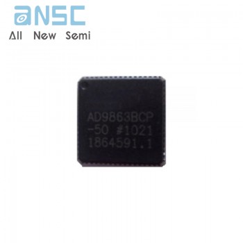
AD9863BCPZ-50 Transceiver for Broadband Applications QFN
SEND
RFQ