+86 135 5637 6665
+852 2632 9637
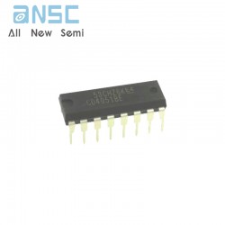
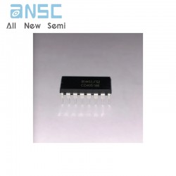
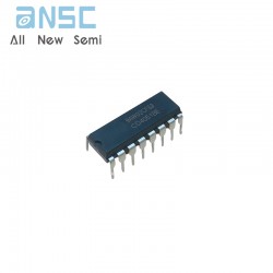
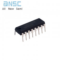
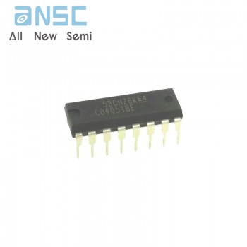
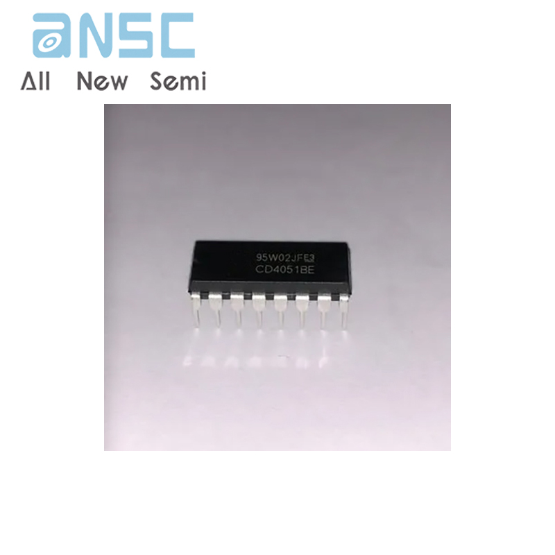
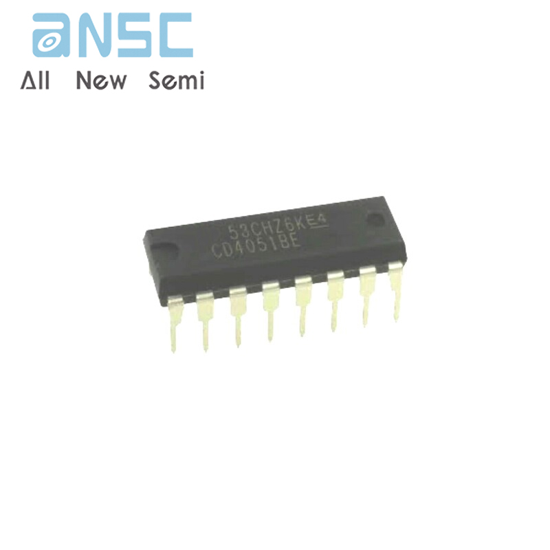
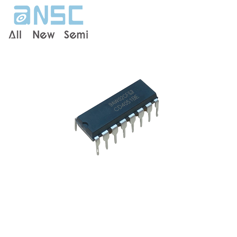
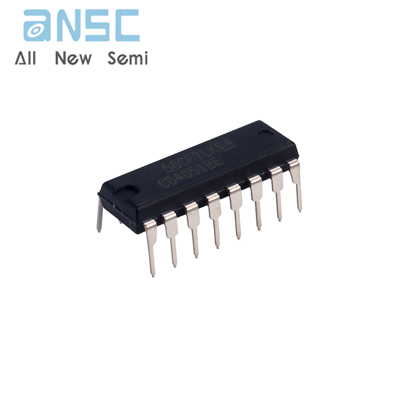
Image shown is a representation only.
Exact specifications should be obtained from the product data sheet.
CD4051BE CMOS Analog Multiplexers/Demultiplexers with Logic Level Conversion DIP-16
The CD4051B is a single 8-Channel multiplexer having three binary control inputs, A, B, and C, and an inhibit input. The three binary signals select 1 of 8 channels to be turned on, and connect one of the 8 inputs to the output.
The CD4052B is a differential 4-Channel multiplexer having two binary control inputs, A and B, and an inhibit input. The two binary input signals select 1 of 4 pairs of channels to be turned on and connect the analog inputs to the outputs.
The CD4053B is a triple 2-Channel multiplexer having three separate digital control inputs, A, B, and C, and an inhibit input. Each control input selects one of a pair of channels which are connected in a single-pole, double-throw configuration.
• Wide Range of Digital and Analog Signal Levels
- Digital . . . . . . . . . . . . . . . . . . . . . . . . . . . . . . 3V to 20V
- Analog. . . . . . . . . . . . . . . . . . . . . . . . . . . . . . . ≤20VP-P
• Low ON Resistance, 125Ω (Typ) Over 15VP-P Signal Input Range for VDD-VEE = 18V
• High OFF Resistance, Channel Leakage of ±100pA (Typ) at VDD-VEE = 18V
• Logic-Level Conversion for Digital Addressing Signals of 3V to 20V (VDD-VSS = 3V to 20V) to Switch Analog Signals to 20VP-P (VDD-VEE = 20V)
• Matched Switch Characteristics, rON = 5Ω (Typ) for VDD-VEE = 15V
• Very Low Quiescent Power Dissipation Under All DigitalControl Input and Supply Conditions, 0.2µW (Typ) at VDD-VSS = VDD-VEE = 10V
• Binary Address Decoding on Chip
• 5V, 10V, and 15V Parametric Ratings
• 100 percent Tested for Quiescent Current at 20V
• Maximum Input Current of 1µA at 18V Over Full Package Temperature Range, 100nA at 18V and 25oC
• Break-Before-Make Switching Eliminates Channel Overlap
• Analog and Digital Multiplexing and Demultiplexing
• A/D and D/A Conversion
• Signal Gating
| Attribute | Attribute value |
| ANSM-Part# | ANSM-CD4051BE |
| Category | Integrated Circuits (ICs) |
| Interface | |
| Analog Switches, Multiplexers, Demultiplexers | |
| Manufacturer | - |
| Series | - |
| Packaging | Tube |
| Part Status | Active |
| Switch Circuit | - |
| Multiplexer/Demultiplexer Circuit | 8:1 |
| Number of Circuits | 1 |
| On-State Resistance (Max) | 240Ohm |
| Channel-to-Channel Matching (螖Ron) | 5Ohm |
| Voltage - Supply, Single (V+) | 3V ~ 20V |
| Voltage - Supply, Dual (V卤) | ±2.5V ~ 9V |
| Switch Time (Ton, Toff) (Max) | - |
| -3db Bandwidth | 20MHz |
| Charge Injection | - |
| Channel Capacitance (CS(off), CD(off)) | 0.2pF, 30pF |
| Current - Leakage (IS(off)) (Max) | 100nA |
| Crosstalk | - |
| Operating Temperature | -55°C ~ 125°C (TA) |
| Mounting Type | Through Hole |
| Package / Case | 16-DIP (0.300", 7.62mm) |
| Supplier Device Package | 16-PDIP |
| Base Product Number | CD4051 |
For more product information, please download the PDF
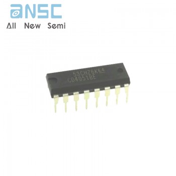
CD4051BE CMOS Analog Multiplexers/Demultiplexers with Logic Level Conversion DIP-16
SEND
RFQ