+86 135 5637 6665
+852 2632 9637
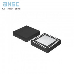
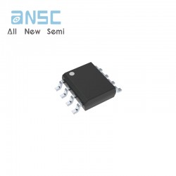
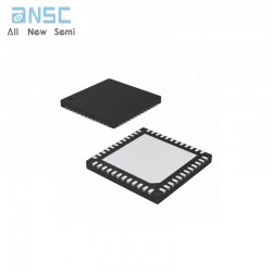
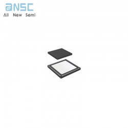
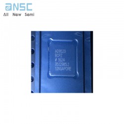
Image shown is a representation only.
Exact specifications should be obtained from the product data sheet.
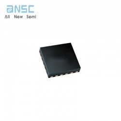
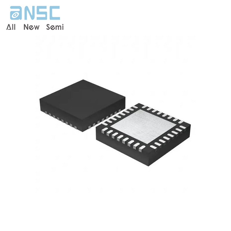
CDCLVD110ARHBT Programmable Low-Voltage 1:10 LVDS Clock Driver 32VQFN spot stock
The CDCLVD110A clock driver distributes one pair ofdifferential LVDS clock inputs (either CLK0 or CLK1)to 10 pairs of differential clock outputs (Q0 to Q9)with minimum skew for clock distribution . TheCDCLVD110A is specifically designed to drive 50-Ωtransmission lines .
When the control enable is high (EN = 1), the 10differential outputs are programmable in that eachoutput can be individually enabled or disabled(3-stated) according to the first 10 bits loaded into theshift register . Once the shift register is loaded, thelast bit selects either CLK0 or CLK1 as the clockinput . However, when EN = 0, the outputs are notprogrammable and all outputs are enabled .
The CDCLVD110A has an improved start-up circuitthat minimizes enabling time in AC - and DC-coupledsystems .
The CDCLVD110A is characterized for operationfrom –40°C to 85°C .
• Low-Output Skew <30 ps (Typical) for Clock Distribution Applications
• Distributes One Differential Clock Input to 10 LVDS Differential Clock Outputs
• VCC Range: 2.5 V ±5%
• Typical Signaling Rate Capability of Up to 1.1 GHz
• Configurable Register (SI/CK) Individually Enables Disables Outputs, Selectable CLK0, CLK0 orCLK1, CLK1 Inputs
• Full Rail-to-Rail Common-Mode Input Range
• Receiver Input Threshold: ± 100 mV
• Available in 32-Pin LQFP and VQFN Package
• Fail-Safe I/O-Pins for VDD = 0 V (Power Down)
• General-Purpose Industrial, Communication and Consumer Applications
| Attribute | Attribute value |
| ANSM-Part# | ANSM-CDCLVD110ARHBT |
| Category | Integrated Circuits (ICs) |
| Clock/Timing | |
| Clock Buffers, Drivers | |
| Manufacturer | - |
| Packaging | Tape & Reel (TR) |
| Cut Tape (CT) | |
| Digi-Reel® | |
| Part Status | Active |
| Type | Fanout Buffer (Distribution), Multiplexer |
| Number of Circuits | 1 |
| Ratio - Input:Output | 2:10 |
| Differential - Input:Output | Yes/Yes |
| Input | LVDS |
| Output | LVDS |
| Frequency - Max | 1.1 GHz |
| Voltage - Supply | 2.375V ~ 2.625V |
| Operating Temperature | -40°C ~ 85°C |
| Mounting Type | Surface Mount |
| Package / Case | 32-VFQFN Exposed Pad |
| Supplier Device Package | 32-VQFN (5x5) |
| Base Product Number | CDCLVD110 |
For more product information, please download the PDF
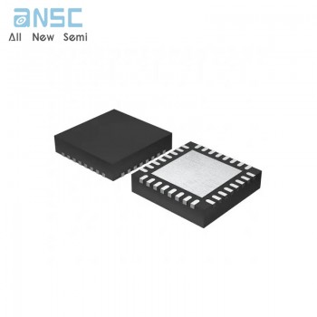
CDCLVD110ARHBT Programmable Low-Voltage 1:10 LVDS Clock Driver 32VQFN spot stock
SEND
RFQ