+86 135 5637 6665
+852 2632 9637
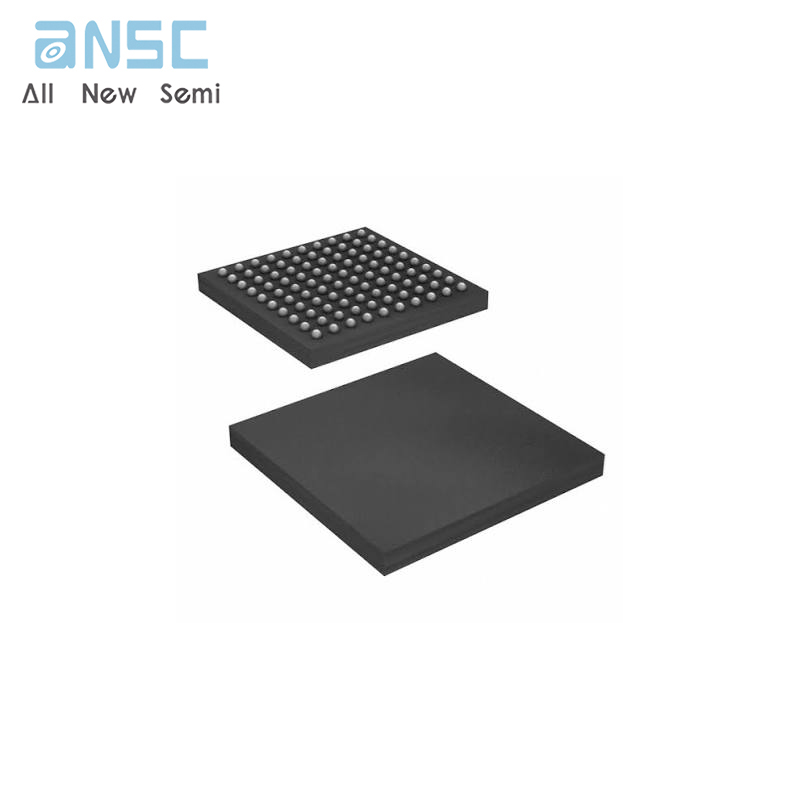
Image shown is a representation only.
Exact specifications should be obtained from the product data sheet.
8V19N490BDGI Jitter Attenuator and Clock Synthesizer 100CABGA spot stock
The 8V19N490 is a fully integrated jitter attenuatorand clock synthesizer designed as a high-performance clock solutionfor conditioning and frequency/phase management of wireless basestation radio equipment boards . The device is optimized to deliverexcellent phase noise performance as required in GSM, WCDMA,LTE, and LTE-A radio board implementations . The device supportsJESD204B subclass 0 and 1 clocks.
A two-stage PLL architecture supports both jitter attenuation andfrequency multiplication . The first stage PLL is the jitter attenuatorand uses an external VCXO for best possible phase noisecharacteristics . The second stage PLL locks on the VCXO-PLLoutput signal and synthesizes the target frequency
The device supports the clock generation of high-frequency clocksfrom the selected VCO and low-frequency synchronization signals(SYSREF). SYSREF signals are internally synchronized to the clocksignals . Delay functions exist for achieving alignment and controlledphase delay between system reference and clock signals and toalign/delay individual output signals . The four redundant inputs aremonitored for activity . Four selectable clock switching modes areprovided to handle clock input failure scenarios . Auto-lock,individually programmable output frequency dividers, and phaseadjustment capabilities are added for flexibility .
The device is configured through a 3-wire SPI interface and reportslock and signal loss status in internal registers and via a lock detect(LOCK) output . Internal status bit changes can also be reported viathe nINT output . The 8V19N490 is ideal for driving converter circuitsin wireless infrastructure, radar/imaging, and instrumentation/medical applications . The device is a member of thehigh-performance clock family from Renesas .
▪ High-performance clock RF-PLL with support for JESD204B
▪ Optimized for low-phase noise: -150dBc/Hz (800kHz offset; 245.76MHz clock)
▪ Integrated phase noise of 80fs RMS typical (12kHz–20MHz)
▪ Dual-PLL architecture
▪ First PLL stage with external VCXO for clock jitter attenuation
▪ Second PLL with internal FemtoClock NG PLL:2949 .12 MHz
▪ Six output channels with a total of 19 outputs, organized in:
— Four JESD204B channels (device clock and SYSREF output) with two, four and six outputs
— One clock channel with two outputs
— One VCXO output
▪ Configurable integer clock frequency dividers
▪ Supported clock output frequencies include: 2949.12, 1474.56,983.04, 491 .52, 245.76, and 122.88MHz
▪ Low-power LVPECL/LVDS outputs support configurable signal amplitude, DC and AC coupling and LVPECL, LVDS line terminations techniques
▪ Phase delay circuits:
— Clock phase delay with 256 steps of 339ps and a range of 0 to 86.466ns
— Individual SYSREF phase delay with 8 steps of 169ps
— Additional individual SYSREF fine phase delay with 25ps steps
— Global SYSREF signal delay with 256 steps of 339ps and a range of 0 to 86.466ns
▪ Redundant input clock architecture with four inputs, including:
— Input activity monitoring
— Manual and automatic, fault-triggered clock selection modes
— Priority controlled clock selection
— Digital holdover and hitless switching
— Differential inputs accept LVDS and LVPECL signals
▪ SYSREF generation modes include internal and external trigger mode for JESD204B
▪ Supply voltage: 3.3V
▪ SPI and control I/O voltage: 1.8V/3 .3V (selectable)
▪ Package: 11 11mm 100-CABGA
▪ Temperature range: -40°C to +85°C
▪ Wireless infrastructure applications: GSM, WCDMA, LTE, LTE-A
▪ Ideal clock driver for jitter-sensitive ADC and DAC circuits
▪ Low-phase noise clock generation
▪ Ethernet line cards
▪ Radar and imaging
▪ Instrumentation and medical
| Attribute | Attribute value |
| ANSM-Part# | ANSM-8V19N490BDGI |
| Category | Integrated Circuits (ICs) |
| Clock/Timing | |
| Clock Generators, PLLs, Frequency Synthesizers | |
| Manufacturer | - |
| Series | FemtoClock® NG |
| Packaging | Tray |
| Part Status | Active |
| DigiKey Programmable | Not Verified |
| Type | Jitter Attenuator |
| PLL | Yes |
| Input | LVDS, LVPECL |
| Output | LVDS, LVPECL |
| Number of Circuits | 1 |
| Ratio - Input:Output | 4:18 |
| Differential - Input:Output | Yes/No |
| Frequency - Max | 2.949GHz |
| Divider/Multiplier | Yes/No |
| Voltage - Supply | 3.3V |
| Operating Temperature | -40°C ~ 85°C |
| Mounting Type | Surface Mount |
| Package / Case | 100-TBGA |
| Supplier Device Package | 100-CABGA (11x11) |
| Base Product Number | 8V19N490 |
For more product information, please download the PDF
8V19N490BDGI Jitter Attenuator and Clock Synthesizer 100CABGA spot stock
SEND
RFQ