
Clock/Timer ICs
Hot-selling and scarce TLC2932AIPW Phase Lock Loop IC 55MHz 1 14-TSSOP spot stock
$0.00
+86 135 5637 6665
+852 2632 9637

Image shown is a representation only.
Exact specifications should be obtained from the product data sheet.
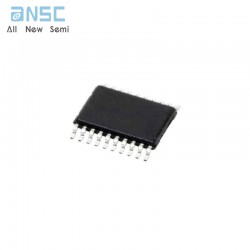
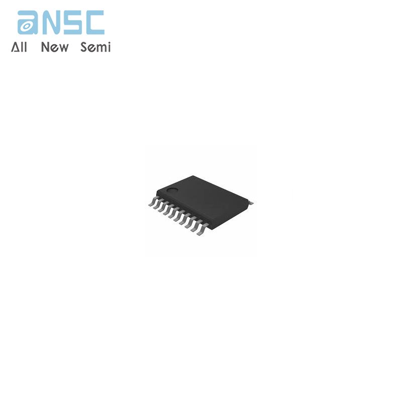
CDCE706PWR PROGRAMMABLE 3-PLL CLOCK SYNTHESIZER/MULTIPLIER/DIVIDER TSSOP20 spot stock
The CDCE706 is one of the smallest and mostpowerful PLL synthesizer/multiplier/dividers availabletoday . Despite its small physical outline, theCDCE706 is very flexible . It has the capability toproduce an almost independent output frequencyfrom a given input frequency .
The input frequency can be derived from anLVCMOS, differential input clock, or single crystal .The appropriate input waveform can be selected viathe SMBus data interface controller .
To achieve an independent output frequency, thereference divider M and the feedback divider N foreach PLL can be set to values from 1 to 511 for theM-divider and from 1 to 4095 for the N-divider . ThePLL-VCO (voltage controlled oscillator) frequencythen is routed from the programmable outputswitching matrix to any of the six outputs . Theswitching matrix includes an additional 7-bitpost-divider (1 to 127) and an inverting logic for eachoutput .
The deep M/N divider ratio allows the generation ofzero-ppm clocks from any reference input frequency(e .g ., 27 MHz).
The CDCE706 includes three PLLs; of those, onesupports spread-spectrum clocking (SSC). PLL1,PLL2, and PLL3 are designed for frequencies up to300 MHz and optimized for zero-ppm applicationswith wide divider factors .
• High-Performance 3:6 PLL-Based Clock Synthesizer/Multiplier/Divider
• User-Programmable PLL Frequencies
• EEPROM Programming Without the Need to Apply High Programming Voltage
• Easy In-Circuit Programming via SMBus Data Interface
• Wide PLL Divider Ratio Allows 0-ppm Output Clock Error
• Clock Inputs Accept a Crystal, a Single-Ended LVCMOS, or a Differential Input Signal
• Accepts Crystal Frequencies From 8 MHz to 54 MHz
• Accepts LVCMOS or Differential Input Frequencies up to 200 MHz
• Two Programmable Control Inputs [S0/S1, A0/A1] for User-Defined Control Signals
• Six LVCMOS Outputs With Output Frequencies up to 300 MHz
• LVCMOS Outputs Can Be Programmed for Complementary Signals
• Free Selectable Output Frequency via Programmable Output Switching Matrix [6×6] Including 7-Bit Post-Divider for Each Output
• PLL Loop Filter Components Integrated
• Low Period Jitter (Typically 60 ps)
• Features Spread-Spectrum Clocking (SSC) for Lowering System EMI
• Programmable Output Slew-Rate Control (SRC) for Lowering System EMI
• 3.3-V Device Power Supply
• Industrial Temperature Range –40°C to 85°C
• Development and Programming Kit for Easy PLL Design and Programming (TI ClockPro Software)
• Packaged in 20-Pin TSSOP
For more product information, please download the PDF
CDCE706PWR PROGRAMMABLE 3-PLL CLOCK SYNTHESIZER/MULTIPLIER/DIVIDER TSSOP20 spot stock
SEND
RFQ