+86 135 5637 6665
+852 2632 9637
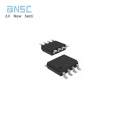
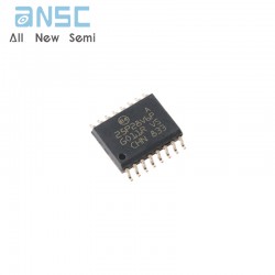
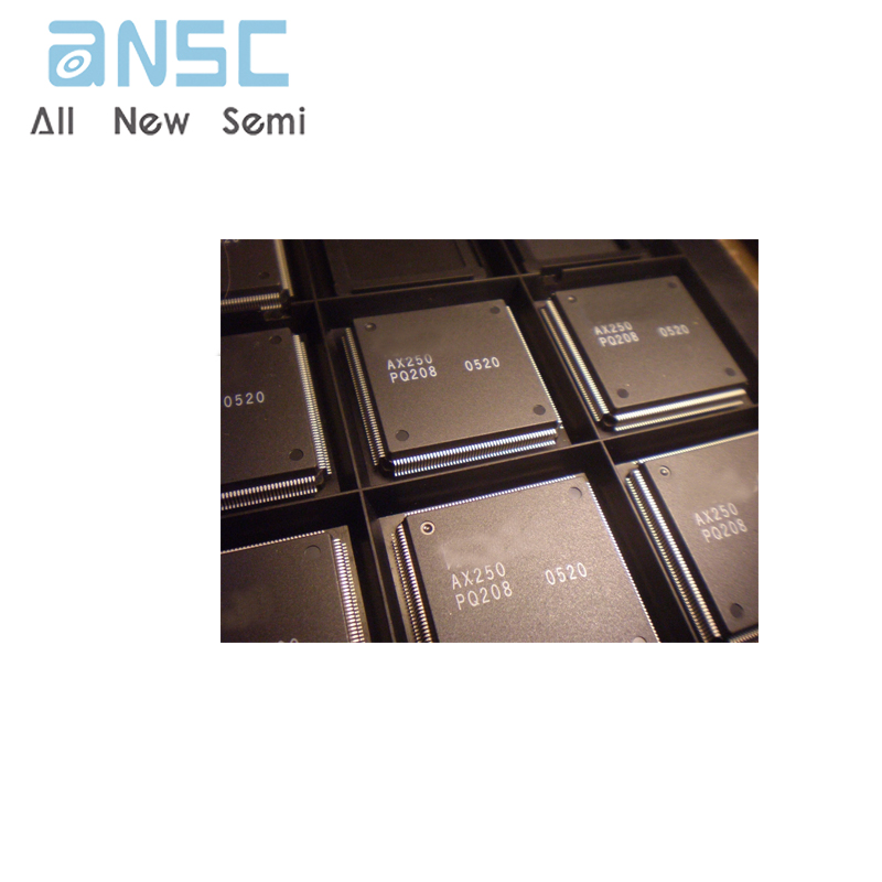
Image shown is a representation only.
Exact specifications should be obtained from the product data sheet.
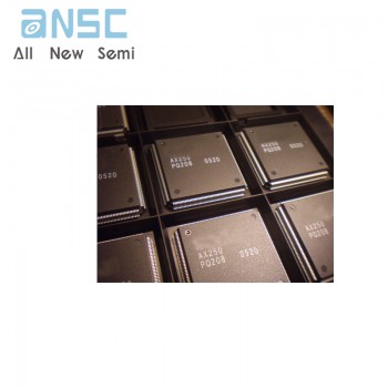
AX250-PQ208 Axcelerator Family FPGAs TQFP spot stock
This datasheet covers Antifuse family of FPGAs and Axcelerator devices, which provides exceptional design security and outstanding performance at densities of up to two million equivalent system gates. Axcelerator devices, which use our AX architecture, have a number of system-level capabilities including segmentable clocks, PLLs, chip-wide highway routing, embedded SRAM (with embedded FIFO control logic), and the capacity to carry logic. Axcelerator devices, which are developed using a CMOS antifuse process technique based on 0.15 µm and seven layers of metal, provide a higher level of performance that was previously limited to ASIC technology.
The following are the features of the Axcelerator devices:
• Single-Chip, Nonvolatile Solution
• Up to 100% Resource Utilization with 100% Pin Locking
• 1.5V Core Voltage for Low Power
• Footprint Compatible Packaging
• Flexible, Multi-Standard I/Os:
– 1.5V, 1.8V, 2.5V, 3.3V mixed voltage operation
– Bank-selectable I/Os—8 banks per chip
– Single-ended I/O standards: LVTTL, LVCMOS, 3.3V PCI, and 3.3V PCI-X
– Differential I/O standards: LVPECL and LVDS
– Voltage-referenced I/O standards: GTL+, HSTL Class 1, SSTL2 Class 1 and 2, and SSTL3 Class 1 and 2
– Registered I/Os
– Hot-swap compliant I/Os (except PCI)
– Programmable slew rate and drive strength on outputs
– Programmable delay and weak pull-up/pull-down circuits on inputs
• Embedded Memory:
– Variable-aspect 4,608-bit RAM blocks (x1, x2, x4, x9, x18, and x36 organizations available)
– Independent, width-configurable read and write ports
– Programmable embedded FIFO control logic
• Segmentable Clock Resources
• Embedded Phase-Locked Loop:
– 14–200 MHz input range
– Frequency synthesis capabilities up to 1 GHz
• Deterministic and User-Controllable Timing
• Unique In-System Diagnostic and Debug Capability with Microchip Silicon Explorer II
• Boundary-Scan Testing Compliant with IEEE Standard 1149.1 (JTAG)
• FuseLock™ Programming Technology Protects Against Reverse Engineering and Design Theft
The following table shows the Axcelerator family product profile.
| Attribute | Attribute value |
| ANSM-Part# | ANSM-AX250-PQ208 |
| Category | Integrated Circuits (ICs) |
| Embedded | |
| FPGAs (Field Programmable Gate Array) | |
| Mfr | - |
| Series | Axcelerator |
| Packaging | Tray |
| Part Status | Obsolete |
| DigiKey Programmable | Not Verified |
| Number of LABs/CLBs | 4224 |
| Total RAM Bits | 55296 |
| Number of I/O | 115 |
| Number of Gates | 250000 |
| Voltage - Supply | 1.425V ~ 1.575V |
| Mounting Type | Surface Mount |
| Operating Temperature | 0°C ~ 70°C (TA) |
| Package / Case | 208-BFQFP |
| Supplier Device Package | 208-PQFP (28x28) |
| Base Product Number | AX250 |
、
For more product information, please download the PDF
AX250-PQ208 Axcelerator Family FPGAs TQFP spot stock
SEND
RFQ