+86 135 5637 6665
+852 2632 9637


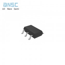
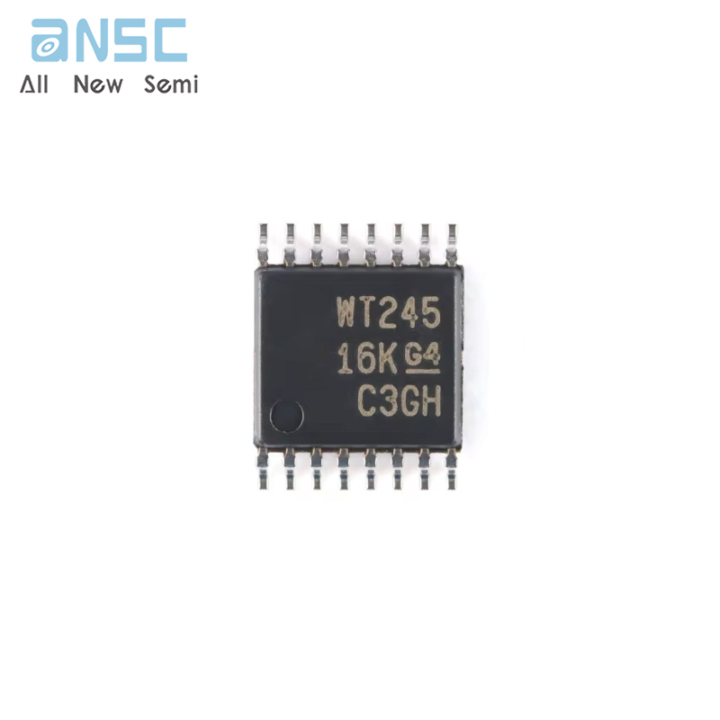
Image shown is a representation only.
Exact specifications should be obtained from the product data sheet.
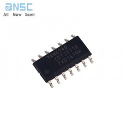
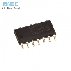
SN74AVC4T245PWR Dual-Bit Bus Transceiver IC TSSOP16 spot stock
This 4-bit noninverting bus transceiver uses two separate configurable power-supply rails. The A port is designed to track V CCA. V CCA accepts any supply voltage from 1.2V to 3.6V. The B port is designed to track VCCB. VCCB accepts any supply voltage from1.2V to 3.6V. The SN74AVC4T245 is optimized to operate with V CCA/VCCB set at 1.4V to 3.6V. It is operational with V CCA/VCCB as low as 1.2V. This allows for universal low-voltage bidirectional translation between any of the 1.2V, 1.5V, 1.8V, 2.5V, and 3.3V voltage nodes.
The SN74AVC4T245 device is designed for asynchronous communication between two data buses. The logic levels of the direction-control (DIR) input and the output-enable (OE) input activate either the B-port outputs or the A-port outputs or place both output ports into the high-impedance mode. The device transmits data from the A bus to the B bus when the B-port outputs are activated, and from the B bus to the A bus when the A-port outputs are activated. The input circuitry on both A and B ports is always active and must have a logic HIGH or LOW level applied to prevent excess ICC and ICCZ.
The SN74AVC4T245 device is designed so that V CCA supplies the control pins (1DIR, 2DIR, 1 OE, and 2 OE).
This device is fully specified for partial-power-down applications using I off. The I off circuitry disables the outputs, preventing damaging current backflow through the device when it is powered down.
The V CC isolation feature is designed so that if either V CC input is at GND, then both ports are in the highimpedance state.
To put the device in the high-impedance state during power up or power down, tie OE to V CC through apullup resistor; the current-sinking capability of the driver determines the minimum value of the resistor.
• Control inputs VIH/VIL levels are referenced to VCCA voltage
• Fully configurable dual-rail design allows each port to operate over the full 1.2V to 3.6V power-supply range
• I/Os Are 4.6V tolerant
• I off supports partial power-down-mode operation
• Maximum data rates:
– 380Mbps (1 .8V to 3 .3V translation)
– 200Mbps (< 1.8V to 3 .3V translation)
– 200Mbps (translate to 2.5V or 1.8V)
– 150Mbps (translate to 1.5V)
– 100Mbps (translate to 1.2V)
• Latch-up performance exceeds 100mA per JESD 78, Class II
• ESD protection exceeds JESD 22:
– 8000V Human-Body Model (A114-A)
– 150V Machine Model (A115-A)
– 1000V Charged-Device Model (C101)
• Personal electronics
• Industrial
• Enterprise
• Telecom
| Attribute | Attribute value |
| ANSM-Part# | ANSM-SN74AVC4T245PWR |
| Category | Integrated Circuits (ICs) |
| Logic | |
| Buffers, Drivers, Receivers, Transceivers | |
| Manufacturer | - |
| Series | 74AVC |
| Packaging | Tape & Reel (TR) |
| Cut Tape (CT) | |
| Digi-Reel® | |
| Part Status | Active |
| Logic Type | Translation Transceiver |
| Number of Elements | 2 |
| Number of Bits per Element | 2 |
| Output Type | 3-State |
| Current - Output High, Low | 12mA, 12mA |
| Voltage - Supply | 1.2V ~ 3.6V |
| Operating Temperature | -40°C ~ 85°C (TA) |
| Mounting Type | Surface Mount |
| Package / Case | 16-TSSOP (0.173", 4.40mm Width) |
| Supplier Device Package | 16-TSSOP |
| Base Product Number | 74AVC4T245 |
For more product information, please download the PDF
WhenCE is HIGH (deselected),the device assumes a standby mode at which the power dissipation can be reduced down to250 µW (typical) with CMOS input levels.

SN74AVC4T245PWR Dual-Bit Bus Transceiver IC TSSOP16 spot stock
SEND
RFQ