+86 135 5637 6665
+852 2632 9637

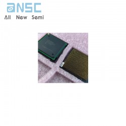
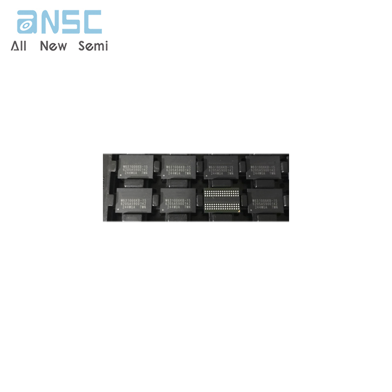
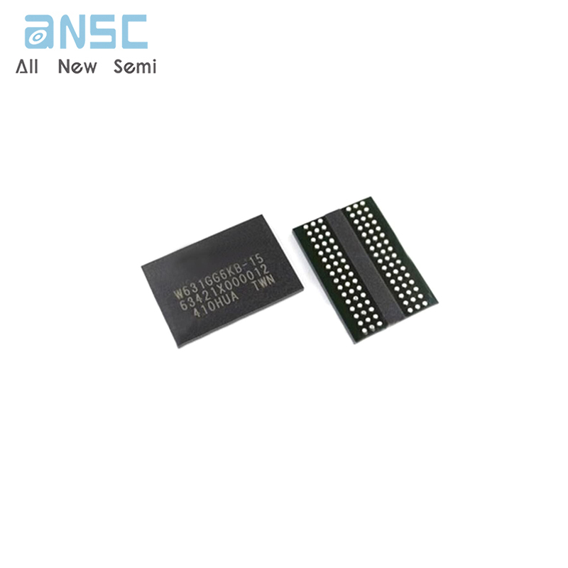
Image shown is a representation only.
Exact specifications should be obtained from the product data sheet.
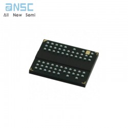
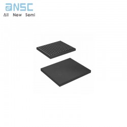
W631GG6KB-15 SDRAM - DDR3 Memory IC 1Gbit Parallel 667 MHz 20 ns 96-WBGA spot stock
The W631GG6KB is a 1G bits DDR3 SDRAM, organized as 8 ,388 ,608 words 8 banks 16 bits. This device achieves high speed transfer rates up to 1866 Mb/sec/pin (DDR3-1866) for various applications. The W631GG6KB is sorted into the following speed grades: -11 , 11I, -12 , 12I, 12J, -15 ,15I and 15J.
The -11 and 11I speed grades are compliant to the DDR3-1866 (13-13-13) specification (The 11 I industrial grade which is guaranteed to support -40°C ≤ TCASE ≤ 95°C).
The -12, 12I and 12J speed grades are compliant to the DDR3-1600 (11-11-11) specification (The 12I industrial grade which is guaranteed to support -40°C ≤ TCASE ≤ 95°C, the 12J industrial plus grade which is guaranteed to support -40°C ≤ TCASE ≤ 105°C).
The -15, 15I and 15J speed grades are compliant to the DDR3-1333 (9-9-9) specification (The 15I industrial grade which is guaranteed to support -40°C ≤ TCASE ≤ 95°C, the 15J industrial plus grade which is guaranteed to support -40°C ≤ TCASE ≤ 105°C).
The W631GG6KB is designed to comply with the following key DDR3 SDRAM features such as posted CAS#, programmable CAS# Write Latency (CWL), ZQ calibration, on die termination and asynchronous reset. All of the control and address inputs are synchronized with a pair of externally supplied differential clocks. Inputs are latched at the cross point of differential clocks (CK rising and CK# falling). All I/Os are synchronized with a differential DQS-DQS# pair in a source synchronous fashion.
Power Supply: VDD , VDDQ = 1.5V ± 0.075V
Double Data Rate architecture: two data transfers per clock cycle
Eight internal banks for concurrent operation
8 bit prefetch architecture
CAS Latency: 6 , 7 , 8, 9 , 10, 11 and 13
Burst length 8 (BL8) and burst chop 4 (BC4) modes: fixed via mode register (MRS) or selectable On The-Fly (OTF)
Programmable read burst ordering: interleaved or nibble sequential
Bi-directional, differential data strobes (DQS and DQS#) are transmitted / received with data
Edge-aligned with read data and center-aligned with write data
DLL aligns DQ and DQS transitions with clock
Differential clock inputs (CK and CK#)
Commands entered on each positive CK edge, data and data mask are referenced to both edges of a differential data strobe pair (double data rate)
Posted CAS with programmable additive latency (AL = 0, CL - 1 and CL - 2) for improved command, address and data bus efficiency
Read Latency = Additive Latency plus CAS Latency (RL = AL + CL)
Auto-precharge operation for read and write bursts
Refresh, Self-Refresh ,Auto Self-refresh (ASR) and Partial array self refresh (PASR)
Precharged Power Down and Active Power Down
Data masks (DM) for write data
| Attribute | Attribute value |
| ANSM-Part# | ANSM-W631GG6KB-15 |
| Category | Integrated Circuits (ICs) |
| Memory | |
| Memory | |
| Mfr | - |
| Packaging | Tray |
| Part Status | Obsolete |
| DigiKey Programmable | Not Verified |
| Memory Type | Volatile |
| Memory Format | DRAM |
| Technology | SDRAM - DDR3 |
| Memory Size | 1Gbit |
| Memory Organization | 64M x 16 |
| Memory Interface | Parallel |
| Clock Frequency | 667 MHz |
| Access Time | 20 ns |
| Voltage - Supply | 1.425V ~ 1.575V |
| Operating Temperature | 0°C ~ 85°C (TC) |
| Mounting Type | Surface Mount |
| Package / Case | 96-TFBGA |
| Supplier Device Package | 96-WBGA (9x13) |
| Base Product Number | W631GG6 |
For more product information, please download the PDF
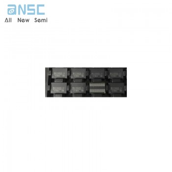
W631GG6KB-15 SDRAM - DDR3 Memory IC 1Gbit Parallel 667 MHz 20 ns 96-WBGA spot stock
SEND
RFQ