+86 135 5637 6665
+852 2632 9637
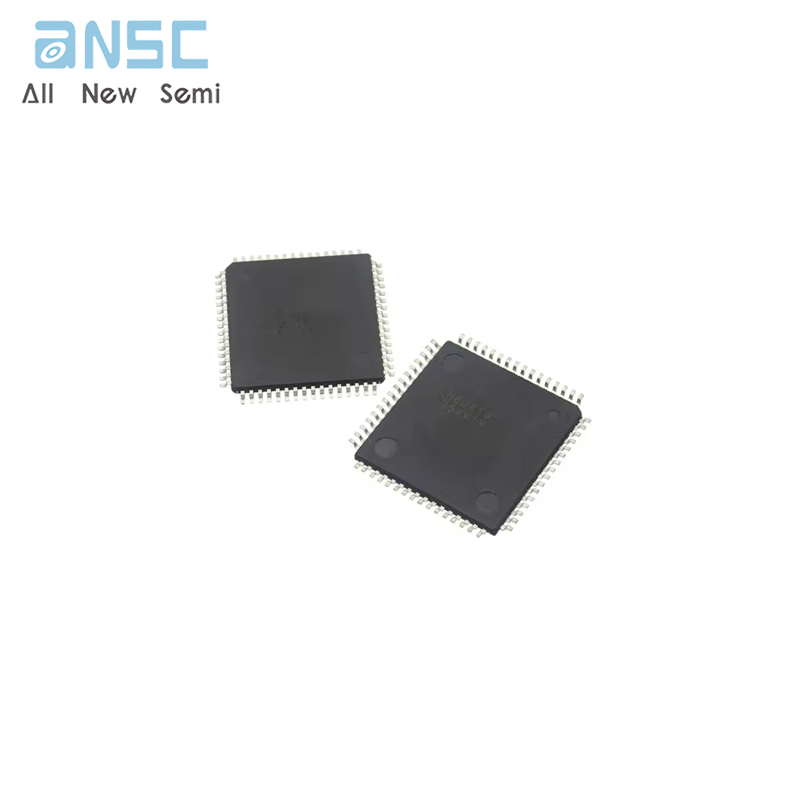
Image shown is a representation only.
Exact specifications should be obtained from the product data sheet.
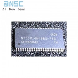
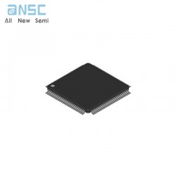
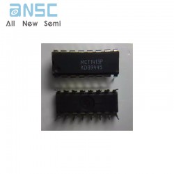
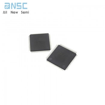
OR2C10A2S208-DB Field-Programmable Gate Arrays IC QFP spot stock
■ High-performance, cost-effective, low-power 0.35 µm CMOS technology (OR2CxxA), 0.3 µm CMOS technology (OR2TxxA), and 0.25 µm CMOS technology (OR2TxxB), (four-input look-up table (LUT) delay less than 1.0 ns with -8 speed grade)
■ High density (up to 43,200 usable, logic-only gates; or 99,400 gates including RAM)
■ Up to 480 user I/Os (OR2TxxA and OR2TxxB I/Os are 5 V tolerant to allow interconnection to both 3.3 V and 5 V devices, selectable on a per-pin basis)
■ Four 16-bit look-up tables and four latches/flip-flops per PFU, nibble-oriented for implementing 4-, 8-, 16-, and/or 32-bit (or wider) bus structures
■ Eight 3-state buffers per PFU for on-chip bus structures
■ Fast, on-chip user SRAM has features to simplify RAM design and increase RAM speed:
— Asynchronous single port: 64 bits/PFU
— Synchronous single port: 64 bits/PFU
— Synchronous dual port: 32 bits/PFU
■ Improved ability to combine PFUs to create larger RAM structures using write-port enable and 3-state buffers
■ Fast, dense multipliers can be created with the multiplier mode (4 x 1 multiplier/PFU):
— 8 x 8 multiplier requires only 16 PFUs
— 30% increase in speed
■ Flip-flop/latch options to allow programmable priority of synchronous set/reset vs. clock enable
■ Enhanced cascadable nibble-wide data path capabilities for adders, subtractors, counters, multipliers, and comparators including internal fast-carry operation
For more product information, please download the PDF
OR2C10A2S208-DB Field-Programmable Gate Arrays IC QFP spot stock
SEND
RFQ